STK551U362A-E 查看數據表(PDF) - ON Semiconductor
零件编号
产品描述 (功能)
生产厂家
STK551U362A-E Datasheet PDF : 15 Pages
| |||
STK551U362A-E
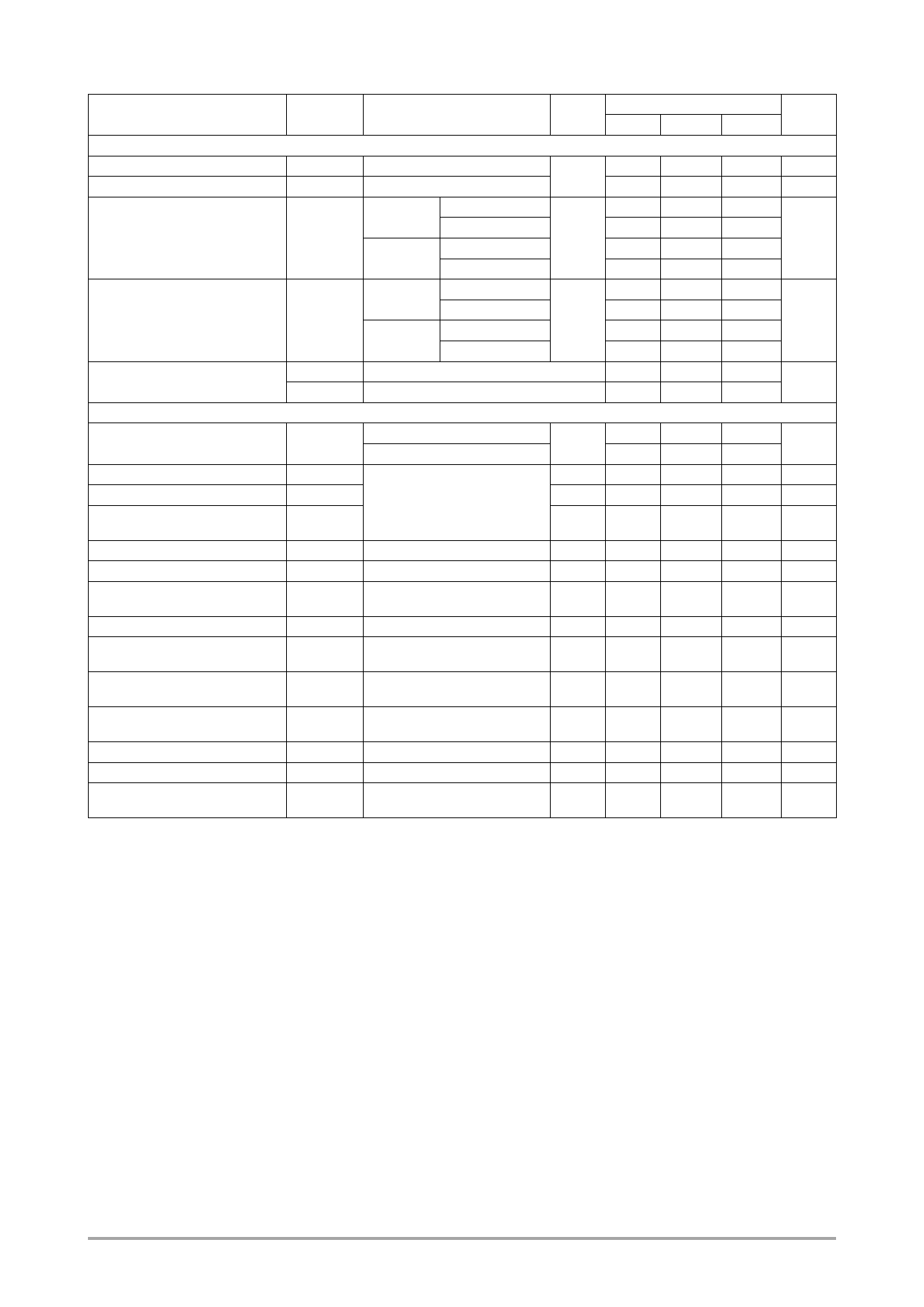
Electrical Characteristics at Tc 25C, VD1, VD2, VD3, VD4 = 15 V
Parameter
Symbol
Conditions
Test
Ratings
circuit min
typ
max
Power output section
Collector-emitter cut-off current
Bootstrap diode reverse current
ICE
IR(BD)
VCE = 600 V
VR(BD)
-
Fig.1
-
Collector to emitter
saturation voltage
Io = 10 A Upper side
-
Tj = 25C Lower side *1
-
VCE(SAT) Io = 5 A
Upper side
Fig.2
-
Tj = 100C Lower side *1
-
Diode forward voltage
Io = 10 A Upper side
-
Tj = 25C Lower side *1
-
VF
Io = 5 A
Upper side
Fig.3
-
Tj = 100C Lower side *1
-
Junction to case
θj-c(T)
IGBT
-
thermal resistance
θj-c(D)
FRD
-
-
0.1
-
0.1
1.8
2.4
2.1
2.7
1.3
-
1.6
-
1.8
2.3
2.1
2.6
1.3
-
1.6
-
-
4
-
5
Control (Pre-driver) section
Pre-driver power dissipation
ID
VD1, 2, 3 = 15 V
VD4 = 15 V
-
0.08
0.4
Fig.4
-
1.6
4
High level Input voltage
Low level Input voltage
Input threshold voltage
hysteresis *1
Logic 1 input leakage current
Logic 0 input leakage current
FAULT terminal input electric
current
FAULT clear time
VCC and VS undervoltage
positive going threshold.
VCC and VS undervoltage
negative going threshold.
VCC and VS undervoltage
hysteresis
Over current protection level
Vin H
Vin L
Vinth(hys)
IIN+
IIN-
IoSD
FLTCLR
VCCUV+
VSUV+
VCCUV-
VSUV-
VCCUVH
VSUVH-
ISD
HIN1, HIN2, HIN3,
LIN1, LIN2, LIN3 to VSS
VIN = +3.3 V
VIN = 0 V
FAULT : ON / VFAULT = 0.1 V
Fault output latch time.
PW = 100 μs, RSD = 0 Ω
Fig.5
2.5
-
0.5
-
-
-
18
10.5
10.3
0.14
18.1
-
-
0.8
100
-
2
-
11.1
10.9
0.2
-
-
0.8
-
143
2
-
80
11.7
11.5
-
22.9
Output level for current monitor ISO
Io = 10 A
Thermistor for substrate
temperature
Rt
Thermistor Resistance
at 25C (Vth)
Reference voltage is “VSS” terminal voltage unless otherwise specified.
*1 : The lower side’s VCE(SAT) and VF include a loss by the shunt resistance
0.31
0.33
0.35
90
100
110
Unit
mA
mA
V
V
C/W
mA
V
V
V
A
A
mA
ms
V
V
A
A
V
kΩ
www.onsemi.com
2
Share Link: 