AP65200MP-13(2014) 查看數據表(PDF) - Diodes Incorporated.
零件编号
产品描述 (功能)
生产厂家
AP65200MP-13 Datasheet PDF : 18 Pages
| |||
AP65200
Application Information (cont.)
Compensation Components
The AP65200 has an external COMP pin through which system stability and transient response can be controlled. COMP pin is the output of the
internal trans-conductance error amplifier. A series capacitor-resistor combination sets a pole-zero combination to control the characteristics of
the control system. The DC gain of the voltage feedback loop is given by:
A VDC
RLOAD
GCS
A VEA
VFB
VOUT
Where VFB is the feedback voltage (0.925V), RLOAD is the load resistor value, GCS is the current sense trans-conductance and AVEA is the error
amplifier voltage gain. The control loop transfer function incorporates two poles one is due to the compensation capacitor (C3) and the output
resistor of error amplifier, and the other is due to the output capacitor and the load resistor. These poles are located at:
fP1
GEA
2 C3 A VEA
fP2
1
2 C2 RLOAD
Where GEA is the error amplifier trans-conductance.
One zero is present due to the compensation capacitor (C3) and the compensation resistor (R3). This zero is located at:
fZ1
1
2 C3 R3
The goal of compensation design is to shape the converter transfer function to get a desired loop gain. The system crossover frequency where
the feedback loop has the unity gain is crucial.
A rule of thumb is to set the crossover frequency to below one-tenth of the switching frequency. Use the following procedure to optimize the
compensation components:
1. Choose the compensation resistor (R3) to set the desired crossover frequency. Determine the R3 value by the following equation:
R3
2 C2 fc
GEA GCS
VOUT
VFB
2
C2 0.1
GEA GCS
fs
VOUT
VFB
Where fC is the crossover frequency, which is typically less than one tenth of the switching frequency.
2. Choose the compensation capacitor (C3) to achieve the desired phase margin set the compensation zero, fZ1, to below one fourth of the
crossover frequency to provide sufficient phase margin. Determine the C3 value by the following equation:
C3
2
R3 fc
Where R3 is the compensation resistor value.
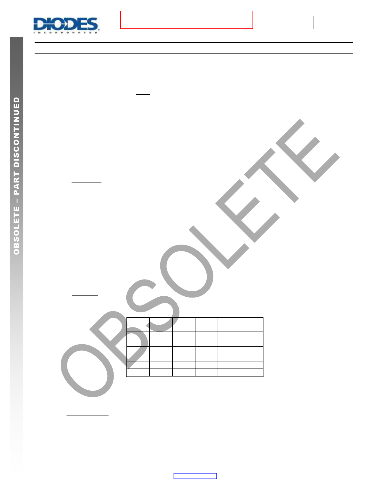
VOUT
(V)
1.2
1.8
2.5
3.3
5
12
CIN/C1
(µF)
22
22
22
22
22
22
COUT/C2
(µF)
47
47
47
47
47
47
RC/R3
(kΩ)
3.24
6.8
6.8
6.8
6.8
6.8
CC/C3
(nF)
6.8
6.8
6.8
6.8
6.8
6.8
L1
(µH)
3.3
3.3
10
10
10
15
Inductor
Table 2 Recommended Component Selection
Calculating the inductor value is a critical factor in designing a buck converter. For most designs, the following equation can be used to calculate
the inductor value;
L
VOUT (VIN
VIN ∆IL
VOUT )
fSW
Where ∆IL is the inductor ripple current.
And fSW is the buck converter switching frequency.
AP65200
Document number: DS35548 Rev. 6 - 2
10 of 18
www.diodes.com
January 2014
© Diodes Incorporated
Share Link: 