AP65200FK-7 查看數據表(PDF) - Diodes Incorporated.
零件编号
产品描述 (功能)
生产厂家
AP65200FK-7 Datasheet PDF : 18 Pages
| |||
PART OBSOLETE
NO ALTERNATE PART
AP65200
Application Information (Cont.)
External Soft Start can be calculated from the formula below:
ISS
C
*
DV
DT
Where:
ISS = Soft Start Current
C = External Capacitor
DV= Change in feedback voltage from 0V to maximum voltage
DT = Soft Start Time
Current Limit Protection
In order to reduce the total power dissipation and to protect the application, AP65200 has cycle-by-cycle current limiting implementation. The
voltage drop across the internal high-side MOSFET is sensed and compared with the internally set current limit threshold. This voltage drop is
sensed at about 30ns after the HS turns on. When the peak inductor current exceeds the set current limit threshold, current limit protection is
activated. During this time the feedback voltage (VFB) drops down. When the voltage at the FB pin reaches 0.3V, the internal oscillator shifts the
frequency from the normal operating frequency of 340kHz to a fold-back frequency of 102kHz. The current limit is reduced to 70% of the nominal
current limit when the part is operating at 102kHz. This low fold-back frequency prevents runaway current.
Undervoltage Lockout (UVLO)
Undervoltage Lockout is implemented to prevent the IC from insufficient input voltages. The AP65200 has a UVLO comparator that monitors the
input voltage and the internal bandgap reference. If the input voltage falls below 4.0V, the AP65200 will latch an undervoltage fault. In this event
the output will be pulled low and power has to be re-cycled to reset the UVLO fault.
Overvoltage Protection
When the AP65200 FB pin exceeds 20% of the nominal regulation voltage of 0.925V, the overvoltage comparator is tripped and the COMP pin
and the SS pin are discharged to GND, forcing the high-side switch off.
Thermal Shutdown
The AP65200 has on-chip thermal protection that prevents damage to the IC when the die temperature exceeds safe margins. It implements a
thermal sensing to monitor the operating junction temperature of the IC. Once the die temperature rises to approximately +160°C, the thermal
protection feature gets activated. The internal thermal sense circuitry turns the IC off, thus preventing the power switch from damage.
A hysteresis in the thermal sense circuit allows the device to cool down to approximately +120°C before the IC is enabled again through soft
start. This thermal hysteresis feature prevents undesirable oscillations of the thermal protection circuit.
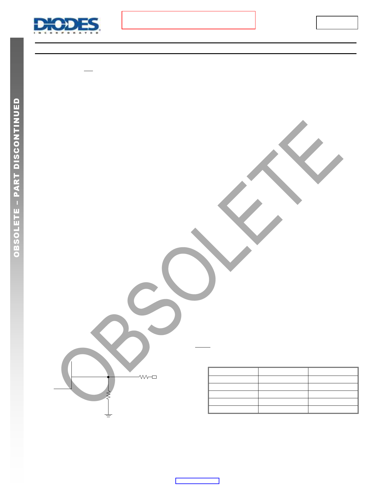
Setting the Output Voltage
The output voltage can be adjusted from 0.925V to 16V using an external resistor divider. Table 1 shows a list of resistor selection for common
output voltages. Resistor R1 is selected based on a design tradeoff between efficiency and output voltage accuracy. For high values of R1 there
is less current consumption in the feedback network. However, the tradeoff is output voltage accuracy due to the bias current in the error
amplifier. R1 can be determined by the following equation:
R1
R2
VOUT
0.925
1
FB
R1
VOUT
R2
Figure 2 Feedback Divider Network
VOUT (V)
5
3.3
2.5
1.8
1.2
R1 (kΩ)
44.2
26.1
16.9
9.53
3
R2 (kΩ)
10
10
10
10
10
Table 1 Resistor Selection for Common Output
Voltages
AP65200
Document number: DS35548 Rev. 9 - 4
9 of 18
www.diodes.com
February 2018
© Diodes Incorporated
Share Link: 