LT1259IN 查看數據表(PDF) - Linear Technology
零件编号
产品描述 (功能)
生产厂家
LT1259IN Datasheet PDF : 12 Pages
| |||
APPLICATIO S I FOR ATIO
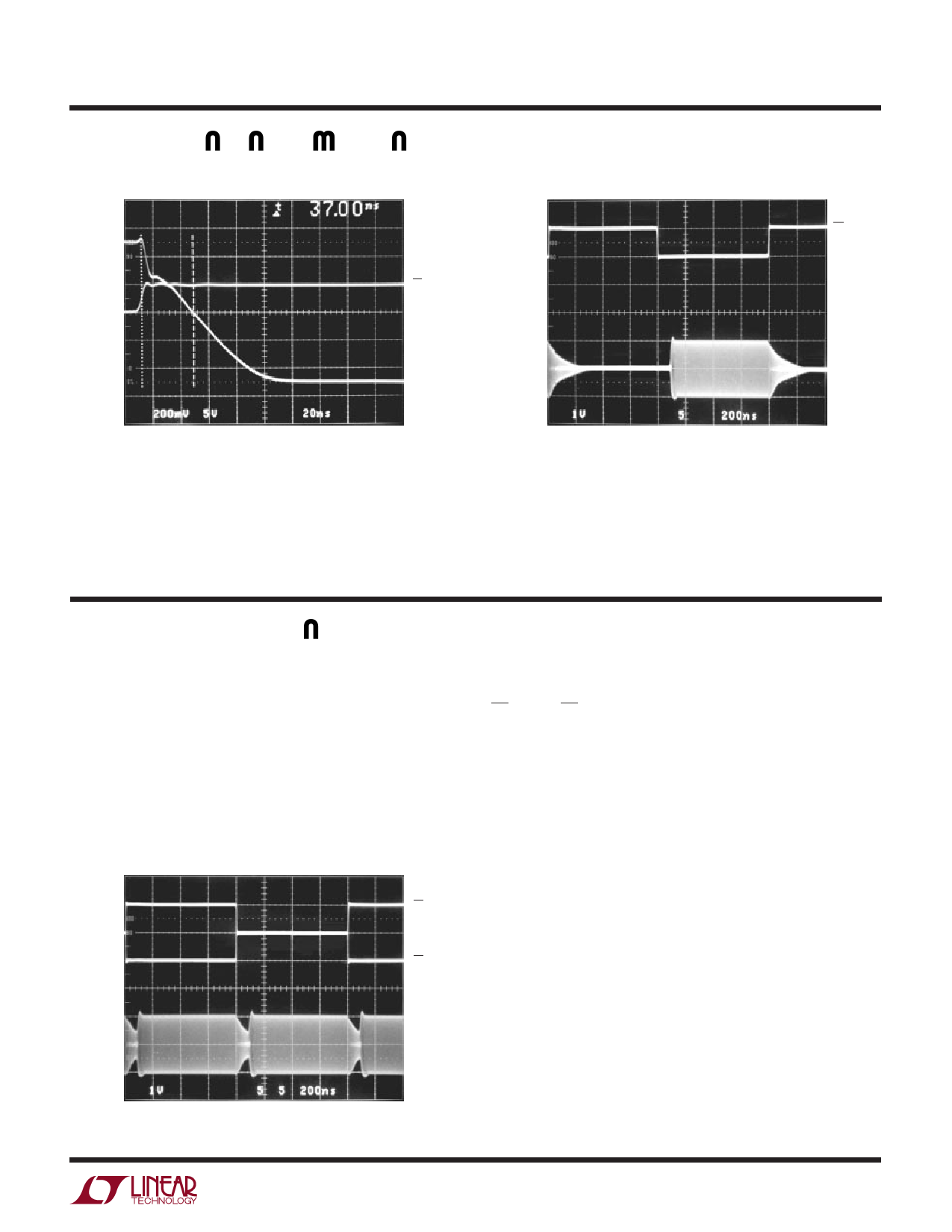
Amplifier Disable Time, AV = 10
EN
LT1259/LT1260
Amplifier Enable/Disable Time, AV = 2
EN
OUTPUT
OUTPUT
VS = ±5V RF = 1k
RL = 150Ω
VIN = 0.1V RG = 110Ω
LT1259/LT1260 • AI05
VS = ±5V
RF = RG = 1.6k
VIN = 2VPP at 2MHz RL = 100Ω
LT1259/LT1260 • AI06
Differential Input Signal Swing
The differential input swing is limited to about ±6V by an
ESD protection device connected between the inputs. In
normal operation, the differential voltage between the
input pins is small, so this clamp has no effect. In the
disabled mode however, the differential swing can be the
same as the input swing, and the clamp voltage will set the
maximum allowable input voltage.
TYPICAL APPLICATIO S
2-Input Video MUX Cable Driver
The application on the first page shows a low cost, 2-
input video MUX cable driver. The scope photo displays
the cable output of a 30MHz square wave driving 150Ω.
In this circuit the active amplifier is loaded by RF and RG
of the disabled amplifier, but in this case it only causes a
1.2% gain error. The gain error can be eliminated by
2-Input Video MUX Switching Response
EN A
EN B
VS = ±5V
RF = RG = 1.6k
VIN A = VIN 2 = 2VPP at 2MHz RL = 100Ω
LT1259/LT1260 • TA03
configuring each amplifier as a unity-gain follower. The
switching time between channels is 100ns when both
EN A and EN B are driven.
2-Input RGB MUX Cable Driver Demonstration Board
A complete 2-input RGB MUX has been fabricated on PC
Demo Board #039A. The board incorporates two LT1260s
with outputs summed through 75Ω back termination
resistors as shown in the schematic. There are several
things to note about Demo Board #039A:
1. The feedback resistors of the disabled LT1260 load
the enabled amplifier and cause a small (1% to 2%)
gain error depending on the values of RF and RG.
Configure the amplifiers as unity-gain followers to
eliminate this error.
2. The feedback node has minimum trace length connect-
ing RF and RG to minimize stray capacitance.
3. Ground plane is pulled away from RF and RG on both
sides of the board to minimize stray capacitance.
9
Share Link: 