AD622(RevC) 查看數據表(PDF) - Analog Devices
零件编号
产品描述 (功能)
生产厂家
AD622 Datasheet PDF : 11 Pages
| |||
AD622
ABSOLUTE MAXIMUM RATINGS1
Supply Voltage . . . . . . . . . . . . . . . . . . . . . . . . . . . . . . . . ± 18 V
Internal Power Dissipation2 . . . . . . . . . . . . . . . . . . . . 650 mW
Input Voltage (Common Mode) . . . . . . . . . . . . . . . . . . . ± VS
Differential Input Voltage . . . . . . . . . . . . . . . . . . . . . . . ± 25 V
Output Short Circuit Duration . . . . . . . . . . . . . . . . Indefinite
Storage Temperature Range (N, R) . . . . . . . –65°C to +125°C
Operating Temperature Range
AD622A . . . . . . . . . . . . . . . . . . . . . . . . . . . – 40°C to +85°C
Lead Temperature Range
(Soldering 10 seconds) . . . . . . . . . . . . . . . . . . . . . . . +300°C
NOTES
1Stresses above those listed under Absolute Maximum Ratings may cause perma-
nent damage to the device. This is a stress rating only; functional operation of the
device at these or any other conditions above those indicated in the operational
section of this specification is not implied. Exposure to absolute maximum rating
conditions for extended periods may affect device reliability.
2Specification is for device in free air:
8-Lead Plastic Package: θJA = 95°C/Watt
8-Lead SOIC Package: θJA = 155°C/Watt
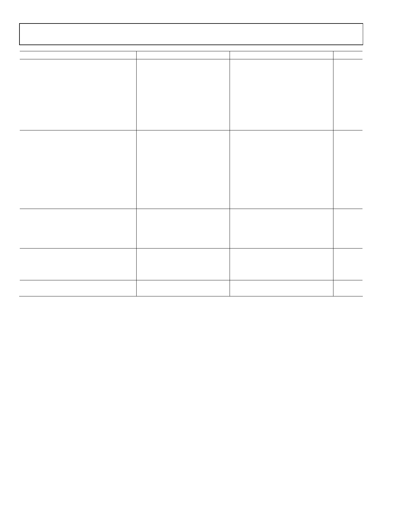
ORDERING GUIDE
Model
Temperature
Range
AD622AN
AD622AR
AD622AR-REEL
AD622AR-REEL7
–40°C to +85°C
–40°C to +85°C
–40°C to +85°C
–40°C to +85°C
*N = Plastic DIP, SO = Small Outline.
Package
Option*
N-8
SO-8
13" Reel
7" Reel
CAUTION
ESD (electrostatic discharge) sensitive device. Electrostatic charges as high as 4000 V readily
accumulate on the human body and test equipment and can discharge without detection.
Although the AD622 features proprietary ESD protection circuitry, permanent damage may
occur on devices subjected to high energy electrostatic discharges. Therefore, proper ESD
precautions are recommended to avoid performance degradation or loss of functionality.
WARNING!
ESD SENSITIVE DEVICE
Typical Characteristics (@ +25؇C, VS = ؎15 V, RL = 2 k⍀, unless otherwise noted)
50
SAMPLE SIZE = 191
40
30
20
10
0
–1.00 –0.80 –0.40
0
0.40
0.80
1.00
OUTPUT OFFSET VOLTAGE – mV
Figure 1. Typical Distribution of Output Offset Voltage
50
SAMPLE SIZE = 383
40
30
20
10
0
60
80
100
120
140
COMMON-MODE REJECTION RATIO – dB
Figure 2. Typical Distribution of Common-Mode Rejection
–4–
REV. C
Share Link: 