GTLP6C817MTC 查看數據表(PDF) - Fairchild Semiconductor
零件编号
产品描述 (功能)
生产厂家
GTLP6C817MTC Datasheet PDF : 7 Pages
| |||
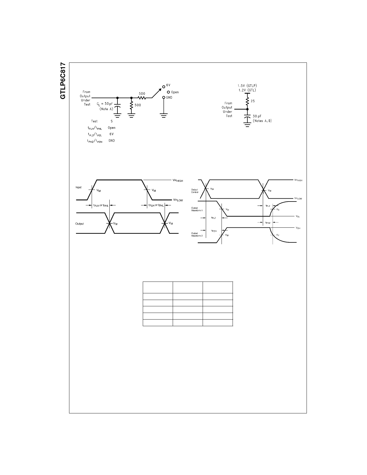
Test Circuit and Timing Waveforms
Test Circuit for A Outputs
Test Circuit for B Outputs
Note A: CL includes probes and jig capacitance.
Voltage Waveform - Propagation Delay Times
Note A: CL includes probes and jig capacitance.
Note B: For B Port CL = 30 pF is used for worst case.
Voltage Waveform - Enable and Disable Times
Output Waveform 1 is for an output with internal conditions such that the
output is LOW except when disabled by the control output
Output Waveforms 2 is for an output with internal conditions such that the
output is HIGH except when disabled by the control output
Input and Measure Conditions
A or LVTTL
Pins
B or GTLP
Pins
VinHIGH
VCC
1.5
VinLOW
0.0
0.0
VM
VCC/2
1.0
VX
VOL + 0.3V
N/A
VY
VOH + 0.3V
N/A
All input pulses have the following characteristics: Frequency = 10MHz, tRISE = tFALL = 2 ns, ZO = 50Ω.
The outputs are measured one at a time with one transition per measurement.
www.fairchildsemi.com
6
Share Link: 