IRU3037 查看數據表(PDF) - International Rectifier
零件编号
产品描述 (功能)
生产厂家
IRU3037 Datasheet PDF : 21 Pages
| |||
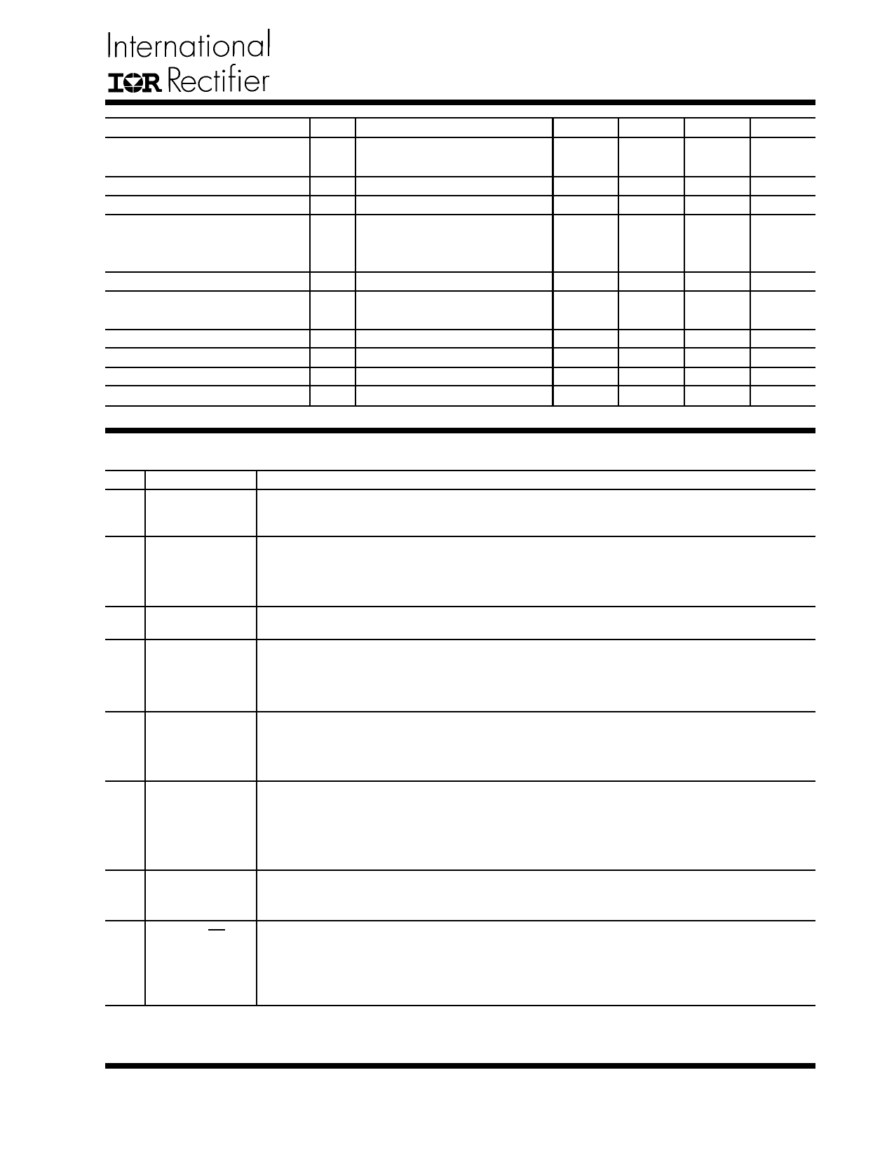
IRU3037/IRU3037A & (PbF)
PARAMETER
Error Amp
Fb Voltage Input Bias Current
Fb Voltage Input Bias Current
Transconductance
Oscillator
Frequency
Ramp-Amplitude Voltage
Output Drivers
Rise Time
Fall Time
Dead Band Time
Max Duty Cycle
Min Duty Cycle
SYM
TEST CONDITION
IFB1 SS=3V, Fb=1V
IFB2 SS=0V, Fb=1V
gm
Freq IRU3037
IRU3037A
VRAMP
Tr CL=1500pF
Tf CL=1500pF
TDB
TON Fb=1V, Freq=200KHz
TOFF Fb=1.5V
MIN TYP MAX UNITS
-0.1
µA
-64
µA
410
600
830 µmho
180
200
220
KHz
345
400
440
1.225 1.25 1.275
V
50
100
ns
50
100
ns
50
150
250
ns
85
90
95
%
0
0
%
PIN DESCRIPTIONS
PIN#
1
PIN SYMBOL PIN DESCRIPTION
Fb
This pin is connected directly to the output of the switching regulator via resistor divider to
provide feedback to the Error amplifier.
2
Vcc
This pin provides biasing for the internal blocks of the IC as well as power for the low side
driver. A minimum of 1µF, high frequency capacitor must be connected from this pin to
ground to provide peak drive current capability.
3
LDrv
Output driver for the synchronous power MOSFET.
4
Gnd
This pin serves as the ground pin and must be connected directly to the ground plane. A
high frequency capacitor (0.1 to 1µF) must be connected from V5 and V12 pins to this pin
for noise free operation.
5
HDrv
Output driver for the high side power MOSFET. Connect a diode, such as BAT54 or 1N4148,
from this pin to ground for the application when the inductor current goes negative (Source/
Sink), soft-start at no load and for the fast load transient from full load to no load.
6
Vc
This pin is connected to a voltage that must be at least 4V higher than the bus voltage of
the switcher (assuming 5V threshold MOSFET) and powers the high side output driver. A
minimum of 1µF, high frequency capacitor must be connected from this pin to ground to
provide peak drive current capability.
7
Comp
Compensation pin of the error amplifier. An external resistor and capacitor network is
typically connected from this pin to ground to provide loop compensation.
8
SS / SD This pin provides soft-start for the switching regulator. An internal current source charges
an external capacitor that is connected from this pin to ground which ramps up the output
of the switching regulator, preventing it from overshooting as well as limiting the input
current. The converter can be shutdown by pulling this pin below 0.5V.
www.irf.com
3
Share Link: 