IPC055N03L3X1SA1 查看數據表(PDF) - Infineon Technologies
零件编号
产品描述 (功能)
生产厂家
IPC055N03L3X1SA1 Datasheet PDF : 4 Pages
| |||
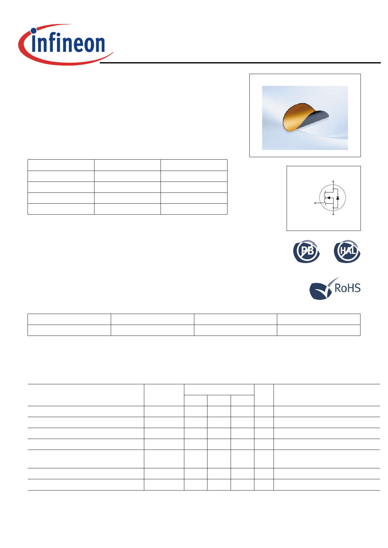
OptiMOS™3PowerMOSTransistorChip
IPC055N03L3
1Description
•N-channelenhancementmode
•FordynamiccharacterizationrefertothedatasheetofIPD031N03LG
•AQL0.65forvisualinspectionaccordingtofailurecatalogue
•ElectrostaticDischargeSensitiveDeviceaccordingtoMIL-STD883C
•Diebond:solderedorglued
•Backsidemetallization:NiVsystem
•Frontsidemetallization:AlCusystem
PowerMOSTransistorChip
Table1KeyPerformanceParameters
Parameter
Value
Unit
V(BR)DSS
RDS(on)
Die size
30
3.11)
3.28 x 1.68
V
mΩ
mm2
Thickness
175
µm
Drain
Gate
Source
Type/OrderingCode
IPC055N03L3
Package
Chip
Marking
not defined
RelatedLinks
-
2ElectricalCharacteristicsonWaferLevel
atTj=25°C,unlessotherwisespecified
Table2
Parameter
Drain-source breakdown voltage
Gate threshold voltage
Zero gate voltage drain current
Gate-source leakage current
Drain-source on- resistance
Reverse diode forward on-voltage
Avalanche energy, single pulse
Symbol
V(BR)DSS
VGS(th)
IDSS
IGSS
RDS(on)
VSD
EAS
Min.
30
1
-
-
-
-
-
-
Values
Typ. Max.
-
-
-
2.2
-
1
-
100
2.72)
1.72)
503)
503)
0.82 1.1
-
90
Unit Note/TestCondition
V VGS=0V,ID=1mA
V
VDS=VGS,ID=250µA
µA VGS=0V,VDS=30V
nA VGS=20V,VDS=0V
mΩ
VGS=4.5V,ID=2.0A
VGS=10V,ID=2.0A
V
VGS=0V,IF=1A
mJ ID =50 A, RGS =25 Ω
1) packaged in a DPAK using Al bond wire (see ref. product)
2)typicalbaredieRDS(on);VGS=10Vwhenusedwith4x500µmAl-wedgedouble-stitchbonding
3) limited by wafer test-equipment
Final Data Sheet
2
Rev.2.5,2014-07-25
Share Link: 