PCA9534D 查看數據表(PDF) - NXP Semiconductors.
零件编号
产品描述 (功能)
生产厂家
PCA9534D Datasheet PDF : 27 Pages
| |||
NXP Semiconductors
PCA9534
8-bit I2C-bus and SMBus low power I/O port with interrupt
6.1.5 Register 3 - Configuration register
This register configures the directions of the I/O pins. If a bit in this register is set, the
corresponding port pin is enabled as an input with high-impedance output driver. If a bit in
this register is cleared, the corresponding port pin is enabled as an output. At reset, the
I/Os are configured as inputs.
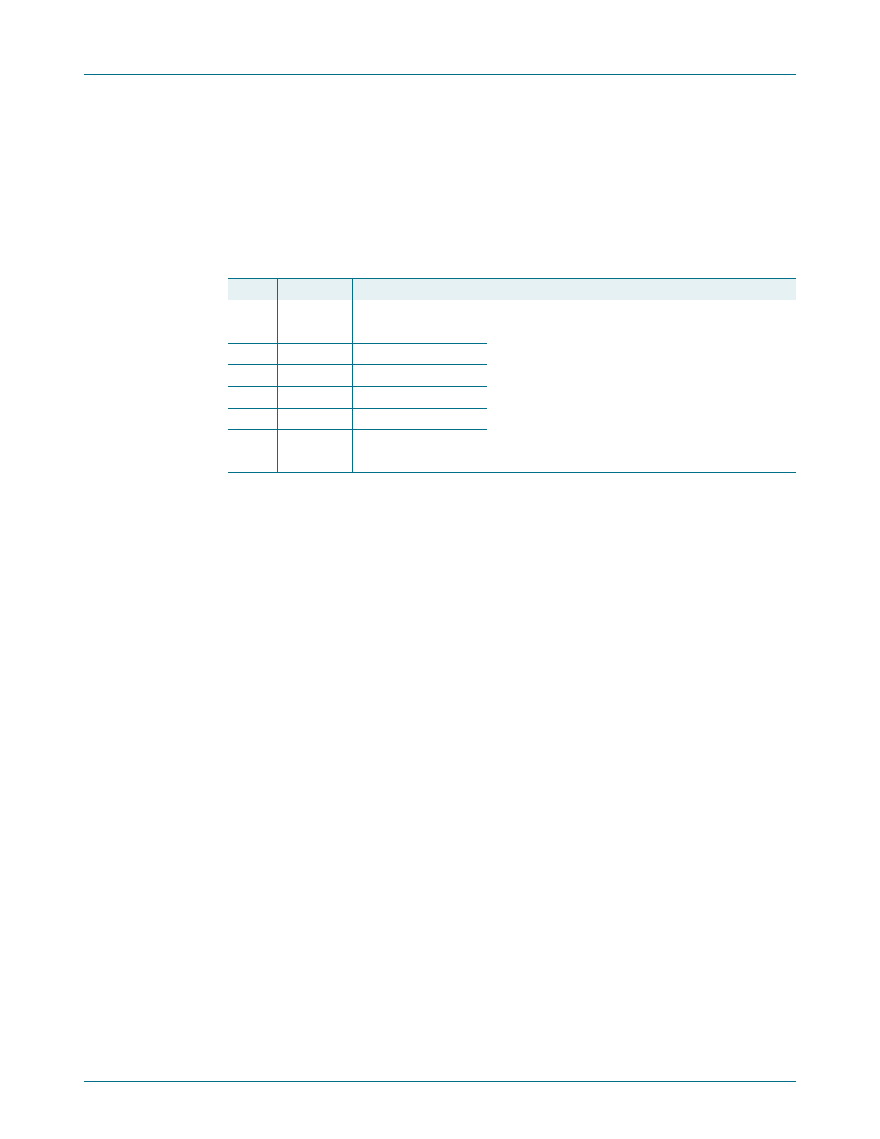
Table 8. Register 3 - Configuration register bit description
Legend: * default value.
Bit Symbol Access Value Description
7
C7
R/W
1*
configures the directions of the I/O pins
6
C6
5
C5
4
C4
R/W
1*
R/W
1*
R/W
1*
0 = corresponding port pin enabled as an output
1 = corresponding port pin configured as input
(default value)
3
C3
R/W
1*
2
C2
R/W
1*
1
C1
R/W
1*
0
C0
R/W
1*
6.2 Power-on reset
When power is applied to VDD, an internal Power-On Reset (POR) holds the PCA9534 in
a reset condition until VDD has reached VPOR. At that point, the reset condition is released
and the PCA9534 registers and state machine will initialize to their default states.
Thereafter, VDD must be lowered below 0.2 V to reset the device.
For a power reset cycle, VDD must be lowered below 0.2 V and then restored to the
operating voltage.
6.3 Interrupt output
The open-drain interrupt output is activated when one of the port pins change state and
the pin is configured as an input. The interrupt is deactivated when the input returns to its
previous state or the Input Port register is read.
Note that changing an I/O from and output to an input may cause a false interrupt to occur
if the state of the pin does not match the contents of the Input Port register.
6.4 I/O port
When an I/O is configured as an input, FETs Q1 and Q2 are off, creating a
high-impedance input. The input voltage may be raised above VDD to a maximum of 5.5 V.
If the I/O is configured as an output, then either Q1 or Q2 is enabled, depending on the
state of the Output Port register. Care should be exercised if an external voltage is applied
to an I/O configured as an output because of the low-impedance paths that exist between
the pin and either VDD or VSS.
PCA9534
Product data sheet
All information provided in this document is subject to legal disclaimers.
Rev. 4 — 7 November 2017
© NXP Semiconductors N.V. 2017. All rights reserved.
7 of 27
Share Link: 