ATXMEGA32A4U 查看數據表(PDF) - Atmel Corporation
零件编号
产品描述 (功能)
生产厂家
ATXMEGA32A4U Datasheet PDF : 339 Pages
| |||
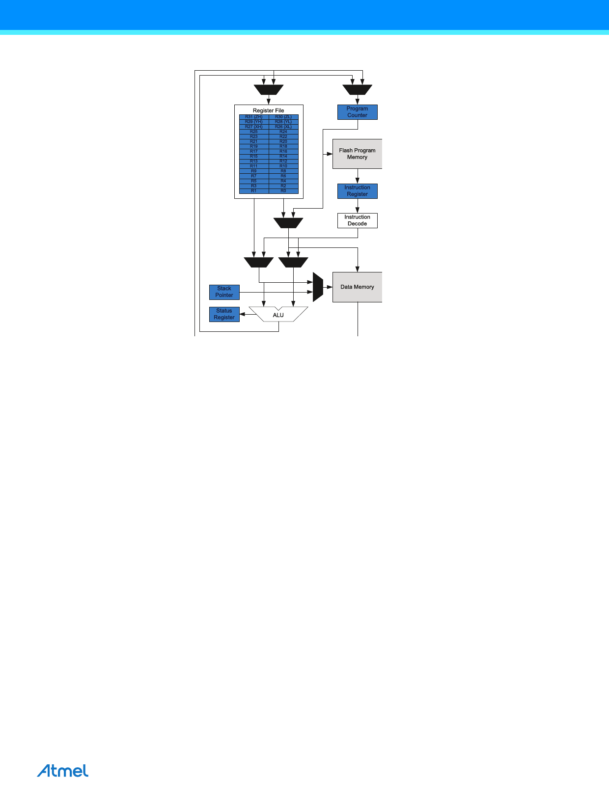
Figure 6-1. Block diagram of the AVR CPU architecture.
The arithmetic logic unit (ALU) supports arithmetic and logic operations between registers or between a constant and
a register. Single-register operations can also be executed in the ALU. After an arithmetic operation, the status
register is updated to reflect information about the result of the operation.
The ALU is directly connected to the fast-access register file. The 32 x 8-bit general purpose working registers all
have single clock cycle access time allowing single-cycle arithmetic logic unit (ALU) operation between registers or
between a register and an immediate. Six of the 32 registers can be used as three 16-bit address pointers for program
and data space addressing, enabling efficient address calculations.
The memory spaces are linear. The data memory space and the program memory space are two different memory
spaces.
The data memory space is divided into I/O registers, SRAM, and external RAM. In addition, the EEPROM can be
memory mapped in the data memory.
All I/O status and control registers reside in the lowest 4KB addresses of the data memory. This is referred to as the
I/O memory space. The lowest 64 addresses can be accessed directly, or as the data space locations from 0x00 to
0x3F. The rest is the extended I/O memory space, ranging from 0x0040 to 0x0FFF. I/O registers here must be
accessed as data space locations using load (LD/LDS/LDD) and store (ST/STS/STD) instructions.
The SRAM holds data. Code execution from SRAM is not supported. It can easily be accessed through the five
different addressing modes supported in the AVR architecture. The first SRAM address is 0x2000.
Data addresses 0x1000 to 0x1FFF are reserved for memory mapping of EEPROM.
The program memory is divided in two sections, the application program section and the boot program section. Both
sections have dedicated lock bits for write and read/write protection. The SPM instruction that is used for self-
programming of the application flash memory must reside in the boot program section. The application section
contains an application table section with separate lock bits for write and read/write protection. The application table
section can be used for safe storing of nonvolatile data in the program memory.
6.4 ALU - Arithmetic Logic Unit
The arithmetic logic unit (ALU) supports arithmetic and logic operations between registers or between a constant and
a register. Single-register operations can also be executed. The ALU operates in direct connection with all 32 general
XMEGA A4U [DATASHEET]
10
Atmel-8387H-AVR-ATxmega16A4U-34A4U-64A4U-128A4U-Datasheet_09/2014
Share Link: 