LT1185(Rev_D) 查看數據表(PDF) - Linear Technology
零件编号
产品描述 (功能)
生产厂家
LT1185 Datasheet PDF : 16 Pages
| |||
UU W U
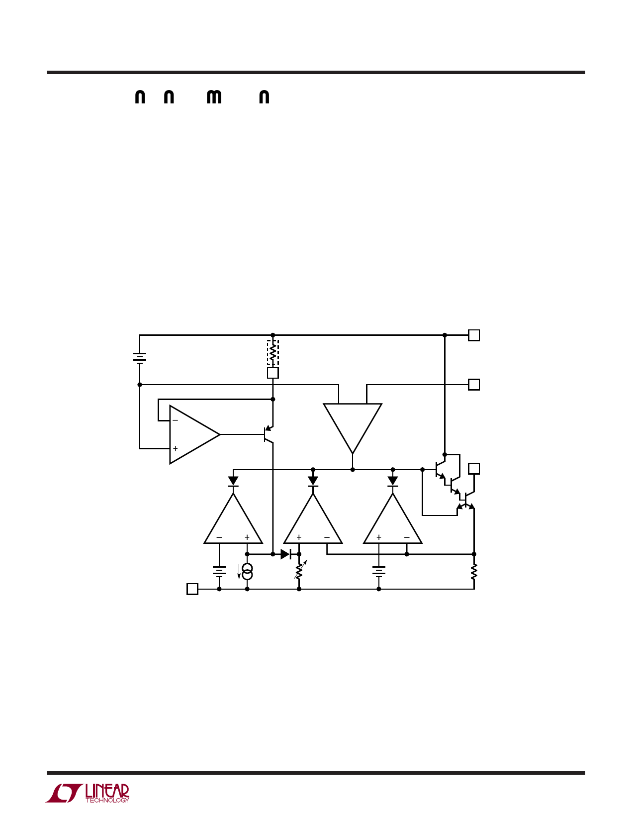
APPLICATIO S I FOR ATIO
Block Diagram
A simplified block diagram of the LT1185 is shown in
Figure 1. A 2.37V bandgap reference is used to bias the
input of the error amplifier A1, and the reference amplifier
A2. A1 feeds a triple NPN pass transistor stage which has
the two driver collectors tied to ground so that the main
pass transistor can completely saturate. This topology
normally has a problem with unlimited current in Q1 and
Q2 when the input voltage is less than the minimum
required to create a regulated output. The standard “fix”
for this problem is to insert a resistor in series with Q1 and
Q2 collectors, but this resistor must be low enough in
value to supply full base current for Q3 under worst-case
LT1185
conditions, resulting in very high supply current when the
input voltage is low. To avoid this situation, the LT1185
uses an auxiliary emitter on Q3 to create a drive limiting
feedback loop which automatically adjusts the drive to Q1
so that the base drive to Q3 is just enough to saturate Q3,
but no more. Under saturation conditions, the auxiliary
emitter is acting like a collector to shunt away the output
current of A1. When the input voltage is high enough to
keep Q3 out of saturation, the auxiliary emitter current
drops to zero even when Q3 is conducting full load current.
VREF
2.37V
–
A2
+
RLIM (EXTERNAL)
REF
–+
A1
Q4
D2
A5
D4
A4
D3
A3
GND
FB
Q1
VOUT
Q2
Q3
300mV
VIN
I1
D1 R1
2µA
350Ω
200mV
Figure 1. Block Diagram
R2
0.055Ω
LT1185 • BD
5
Share Link: 