AN78M06NSP 查看數據表(PDF) - Panasonic Corporation
零件编号
产品描述 (功能)
生产厂家
AN78M06NSP Datasheet PDF : 13 Pages
| |||
AN78MxxNSP Series
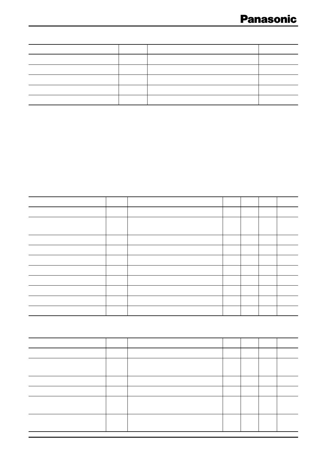
I Absolute Maximum Ratings
Parameter
Symbol
Range
Unit
Supply voltage *2
VCC
35
V
Supply current *3
ICC
mA
Power dissipation *4
PD
mW
Operating ambient temperature *1
Topr
−30 to +85
°C
Storage temperature *1
Tstg
−55 to +150
°C
Note) 1. *1: Except for the operating ambient temperature and storage temperature, all ratings are for Ta = 25°C.
*2: When VCC of 35 V is applied, the overvoltage protection of ASO protection circuit may shut off the output.
*3: Since this IC has incorporated a current limiter, the current value does not exceed the rating.
*4: When Tj exceeds 150°C (designed value), the internal circuit cuts off the output. Note that the relationship between IC
power dissipation and the ambient temperature must follow the derating curve.
2. This IC is not suitable for car electronics equipment.
I Electrical Characteristics at Ta = 25°C
• AN78M05NSP (5 V type)
The specified condition Tj = 25°C means that the test should be carried out within so short a test time (within 10 ms)
that the characteristic value drift due to the chip junction temperature rise can be ignored.
Unless otherwise specified, VI = 10 V, IO = 350 mA, CI = 0.33 µF and CO = 0.1 µF
Parameter
Symbol
Conditions
Min Typ Max Unit
Output voltage
VO1 Tj = 25°C
4.8 5 5.2 V
Output voltage tolerance
VO2 VI = 7.5 V to 20 V, IO = 5 mA to 350 mA 4.75 5.25 V
Tj = 25°C
Line regulation 1
REGIN1 VI = 7.5 V to 25 V, Tj = 25°C
3 100 mV
Line regulation 2
REGIN2 VI = 8 V to 25 V, Tj = 25°C
1 50 mV
Load regulation 1
REGL1 IO = 5 mA to 500 mA, Tj = 25°C
20 100 mV
Load regulation 2
REGL2 IO = 5 mA to 200 mA, Tj = 25°C
10 50 mV
Bias current
IBias Tj = 25°C
4
6 mA
Bias current fluctuation to input ∆IBias(IN) VI = 8 V to 25 V, Tj = 25°C
0.8 mA
Bias current fluctuation to load ∆IBias(L) IO = 5 mA to 350 mA, Tj = 25°C
0.5 mA
Ripple rejection ratio
RR VI = 8 V to 18 V, IO = 100 mA, f = 120 Hz 62 dB
• Design reference data
Note) The characteristics listed below are theoretical values based on the IC design and are not guaranteed.
Parameter
Symbol
Conditions
Min Typ Max Unit
Output noise voltage
VNO f = 10 Hz to 100 kHz
Minimum input/output voltage VDIF(min) IO = 500 mA, Tj = 25°C
difference
40 µV
2
V
Output short-circuit current
Peak output current
Output voltage temperature
coefficient
IO(Short) VI = 35 V, Tj = 25°C
IO(Peak) Tj = 25°C
∆VO / Ta IO = 5 mA, Tj = 0°C to 125°C
300 mA
1 000 mA
− 0.5 mV/°C
Thermal protection operating
temperature
Tj(TH) IO = 5 mA
150 °C
2
SFF00012BEB
Share Link: 