RT8105 查看數據表(PDF) - Richtek Technology
零件编号
产品描述 (功能)
生产厂家
RT8105 Datasheet PDF : 12 Pages
| |||
RT8105
Therefore the ESR can be determined for a given output
voltage ripple requirement.
Input Capacitor Selection
The selection of input capacitor depends on the maximum
ripple current capability. Referred to Figure 1, the buck
converter draws pulsed current from the input capacitor
during S1 is turned on. RMS value of the ripple current
flowing through the input capacitor can be expressed as
follows :
Irms = IOUT D(1− D) (A)
The input capacitor must be able to handle this RMS
current. It is recommended to add ceramic capacitor and
placed physically close to the drain of the high side
MOSFET. This can effectively reduce the input ripple
voltage.
Control Loop Stability
RT8105 utilizes operational transconductance amplifier
(OTA) as the error amplifier and implements the
compensation network internally. Figure 4 shows the
internal Type II compensator, which provides two poles
and one zero to the control loop.
GM
VOUT
C1
C2
R1
Figure 4. Internal Type II Compensator
One of the poles is located at low frequency to increase
the low frequency gain to improve the DC regulation
accuracy. The location of the other pole and the single
zero can be calculated as follows :
FZ
=
2π
1
;
× R1× C2
FP
=
2π
1
×
R1×
⎛
⎜⎝
C1×
C1+
C2
C2
⎞
⎟⎠
The transconductance and the internal compensation
values are : GM = 0.2mA/V, R1 ≈ 75kΩ, C1 ≈ 2.5nF,
C2 ≈ 10pF.
The gain of the internal compensator at middle frequency
can be calculated as follows :
Gmid-freq. = GM x R1
www.richtek.com
10
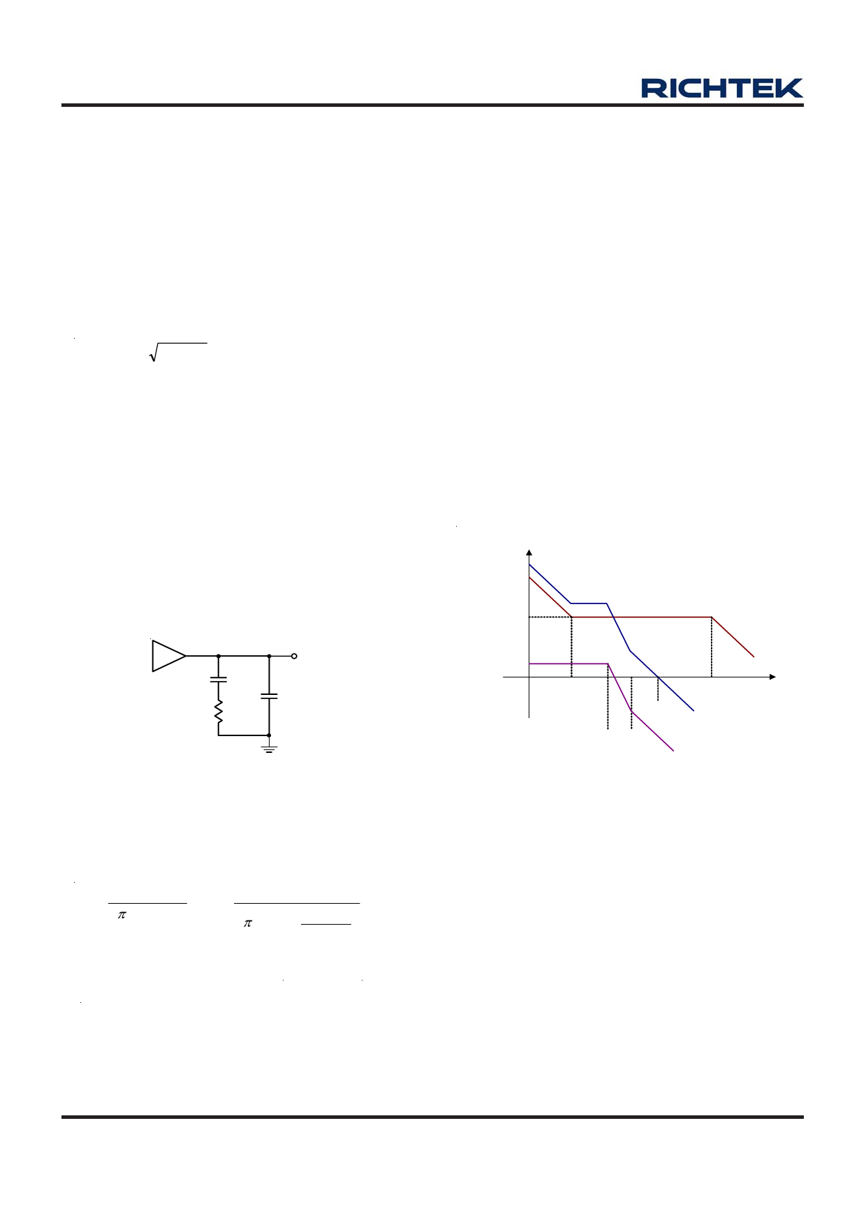
Figure 5 illustrates the system Bode plot. The close loop
gain is the sum of the modulation gain and the
compensation gain. The goal is to obtain the required
crossover frequency with sufficient phase margin. The
crossover frequency is preferred to be 1/10 to 1/5 of the
switching frequency. The preferred phase margin is greater
than 45°.
Because RT8105 utilizes internal compensation, the
location of FZ, FP and the gain at mid-frequency provided
by the compensator are fixed. Therefore the inductance,
output capacitance and especially the ESR of the output
capacitor should be carefully selected to avoid stability
issue. The ESR can not be too small, or the system will
have stability problem. If the location of the zero contributed
by ESR is far away from that of the LC double pole, the
system will not have sufficient phase margin. It is
recommended to choose output capacitor with proper ESR
value to meet the stability requirement.
Gain
(dB)
GM•R1•
(voltage
divider ration)
Compensator
FZ
FP
Freq.
(log scale)
FCROSS
Close Loop
FLC FESR
Modulator
Figure 5. System Bode Plot
PCB Layout Considerations
PCB layout is critical to high-current high-frequency
switching converter design. A good layout can help the
controller to function properly and obtain better
performance. On the other hand, the circuit may have more
power loss, pool performance and even malfunction if
without a carefully layout. In order to obtain better
performance, the general guidelines of PCB layout are
listed as follows.
` Power stage components should be placed first. Place
the input bulk capacitors close to the high side power
MOSFETs, and then locate the output inductor then
finally the output capacitors.
DS8105-03 April 2011
Share Link: 