RT8105 查看數據表(PDF) - Richtek Technology
零件编号
产品描述 (功能)
生产厂家
RT8105 Datasheet PDF : 12 Pages
| |||
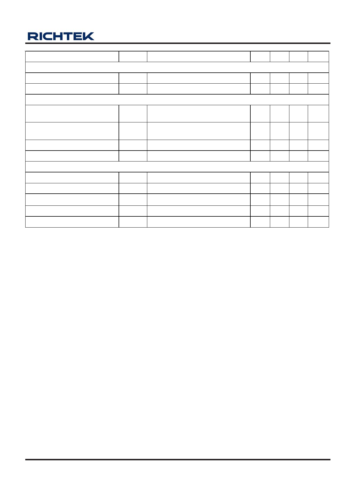
RT8105
Parameter
Error Amplifier (GM)
Symbol
Test Conditions
Min Typ Max Unit
E/A Transconductance
gm
Open Loop DC Gain
AO
PWM Controller Gate Drivers (VCC = 12V)
Upper Gate Source
IUGATE
Upper Gate Sink
Lower Gate Source
Lower Gate Sink
Protection
RUGATE
ILGATE
RLGATE
VBOOT − VPHASE = 12V,
VUGATE − VPHASE = 6V
VBOOT − VPHASE = 12V,
VUGATE − VPHASE = 1V
VCC = 12V, VLGATE = 6V
VCC = 12V, VLGATE = 1V
-- 0.2 -- ms
-- 90 -- dB
0.6 1
--
A
--
4
8
Ω
0.6 1
--
A
--
3
5
Ω
FB Under-Voltage Trip
Δ FBUVT
OC Current Source
IOC
Pre-OVP Threshold (Before POR) VOVP1
OVP Threshold (After POR)
VOVP2
Soft-Start Interval
TSS
FB Falling
VPHASE = 0V
VCC = 3V, Sweep VFB
VCC = 5V, Sweep VFB
70 75 80 %
35 40 45 μA
-- 1.1 1.3 V
1 1.3 1.5 V
-- 3.5 -- ms
Note 1. Stresses listed as the above "Absolute Maximum Ratings" may cause permanent damage to the device. These are for
stress ratings. Functional operation of the device at these or any other conditions beyond those indicated in the
operational sections of the specifications is not implied. Exposure to absolute maximum rating conditions for extended
periods may remain possibility to affect device reliability.
Note 2. θJA is measured in the natural convection at TA = 25°C on a low effective thermal conductivity test board of
JEDEC 51-3 thermal measurement standard.
Note 3. Devices are ESD sensitive. Handling precaution is recommended.
Note 4. The device is not guaranteed to function outside its operating conditions.
DS8105-03 April 2011
www.richtek.com
5
Share Link: 