ADDS-21160M-EZLITE 查看數據表(PDF) - Analog Devices
零件编号
产品描述 (功能)
生产厂家
ADDS-21160M-EZLITE Datasheet PDF : 44 Pages
| |||
AD15700
Driver Amplifier Choice
Although the ADC is easy to drive, the driver amplifier needs to
meet at least the following requirements:
∑ The driver amplifier and the ADC analog input circuit
must be able, together, to settle for a full-scale step of the
capacitor array at a 16-bit level (0.0015%).
∑ The noise generated by the driver amplifier needs to be kept
as low as possible in order to preserve the SNR and transition
noise performance of the ADC. The noise coming from the
driver is first scaled down by the resistive scaler according
to the analog input voltage range used, and is then filtered
by the ADC analog input circuit one-pole, low-pass filter
made by (R/2 + R1) and CS. The SNR degradation due to
the amplifier is:
Ê
Á
SNRLOSS
= log
Á
Á
Á
ËÁÁ
ˆ
˜
28
˜
784 +
p
2
f–3
dB
Ê
ËÁ
2.5 N eN
FSR
ˆ2
¯˜
˜
˜
¯˜˜
where:
f–3 dB is the –3 dB input bandwidth in MHz of the ADC
(9.6 MHz) or the cutoff frequency of the input filter if
any is used (0 V to 2.5 V range).
N is the noise factor of the amplifier (1 if in buffer
configuration).
eN is the equivalent input noise voltage of the op amp
in nV/÷Hz.
FSR is the full-scale span (i.e., 5 V for ± 2.5 V range).
For instance, when using the 0 V to 5 V range, a driver like
the AD15700’s internal op amp, with an equivalent input
noise of 15 nV/÷Hz and configured as a buffer, followed by
a 3.2 MHz RC filter, the SNR degrades by about 1.3 dB.
∑ The driver needs to have a THD performance suitable
to that of the ADC. Figure 11 gives the THD versus
frequency that the driver should preferably exceed.
Voltage Reference Input
The ADC uses an external 2.5 V voltage reference. The voltage
reference input REF of the ADC has a dynamic input impedance.
Therefore, it should be driven by a low impedance source with
an efficient decoupling between REF and REFGND inputs. This
decoupling depends on the choice of the voltage reference, but
usually consists of a low ESR tantalum capacitor connected to the
REF and REFGND inputs with minimum parasitic inductance.
47 mF is an appropriate value for the tantalum capacitor when
used with one of the recommended reference voltages:
∑ The low noise, low temperature drift ADR421 or AD780
voltage references
∑ The low power ADR291 voltage reference
∑ The low cost AD1582 voltage reference
Care should also be taken with the reference temperature coefficient
of the voltage reference, which directly affects the full-scale
accuracy if this parameter matters. For instance, a ± 15 ppm/∞C
tempco of the reference changes the full scale by ± 1 LSB/∞C.
Scaler Reference Input (Bipolar Input Ranges)
When using the ADC with bipolar input ranges, a buffer amplifier
is required to isolate the REFIN pin from the signal dependent
current in the AIN pin. A high speed op amp can be used with a
single 5 V power supply without degrading the performance of
the ADC. The buffer must have good settling characteristics and
provide low total noise within the input bandwidth of the ADC.
Power Supply
The ADC uses three sets of power supply pins: an analog 5 V
supply AVDD, a digital 5 V core supply DVDD, and a digital
input/output interface supply OVDD. The OVDD supply allows
direct interface with any logic working between 2.7 V and 5.25 V.
To reduce the number of supplies needed, the digital core (DVDD)
can be supplied through a simple RC filter from the analog
supply. The ADC is independent of power supply sequencing and
thus free from supply voltage induced latchup. Additionally, it is
very insensitive to power supply variations over a wide frequency
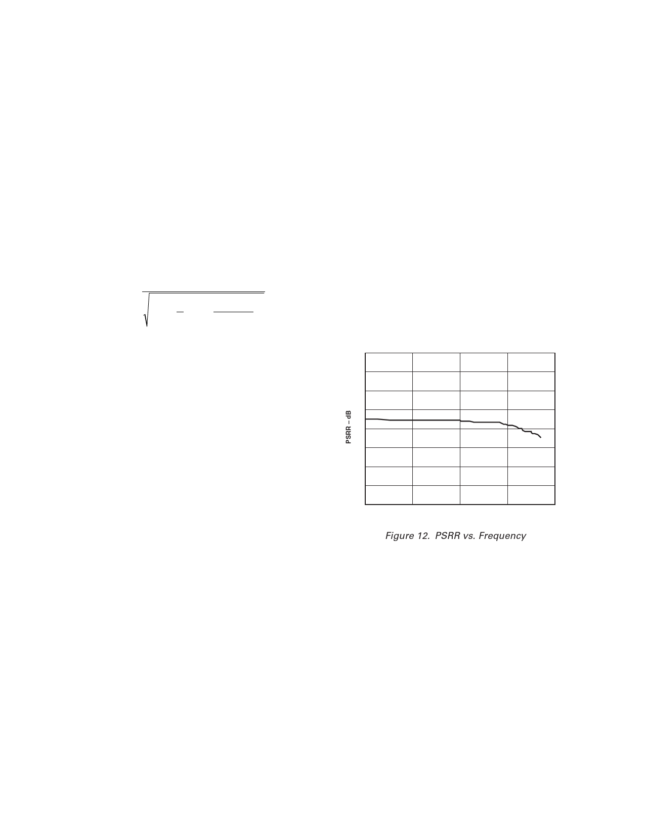
range, as shown in Figure 12.
75
70
65
60
55
50
45
40
35
1
10
100
1000
FREQUENCY – kHz
Figure 12. PSRR vs. Frequency
10000
POWER DISSIPATION
In impulse mode, the ADC automatically reduces its power
consumption at the end of each conversion phase. During the
acquisition phase, the operating currents are very low, which
allows a significant power savings when the conversion rate is
reduced, as shown in Figure 13. This feature makes the ADC
ideal for very low power battery applications.
This does not take into account the power, if any, dissipated by
the input resistive scaler, which depends on the input voltage
range used and the analog input voltage even in power-down
mode. There is no power dissipated when the 0 V to 2.5 V is
used or when both the analog input voltage is 0 V and a unipolar
range, 0 V to 5 V or 0 V to 10 V, is used.
It should be noted that the digital interface remains active even
during the acquisition phase. To reduce the operating digital
supply currents even further, the digital inputs need to be driven
close to the power rails (i.e., DVDD and DGND) and OVDD
should not exceed DVDD by more than 0.3 V.
–30–
REV. A
Share Link: 