ADDS-21160M-EZLITE 查看數據表(PDF) - Analog Devices
零件编号
产品描述 (功能)
生产厂家
ADDS-21160M-EZLITE Datasheet PDF : 44 Pages
| |||
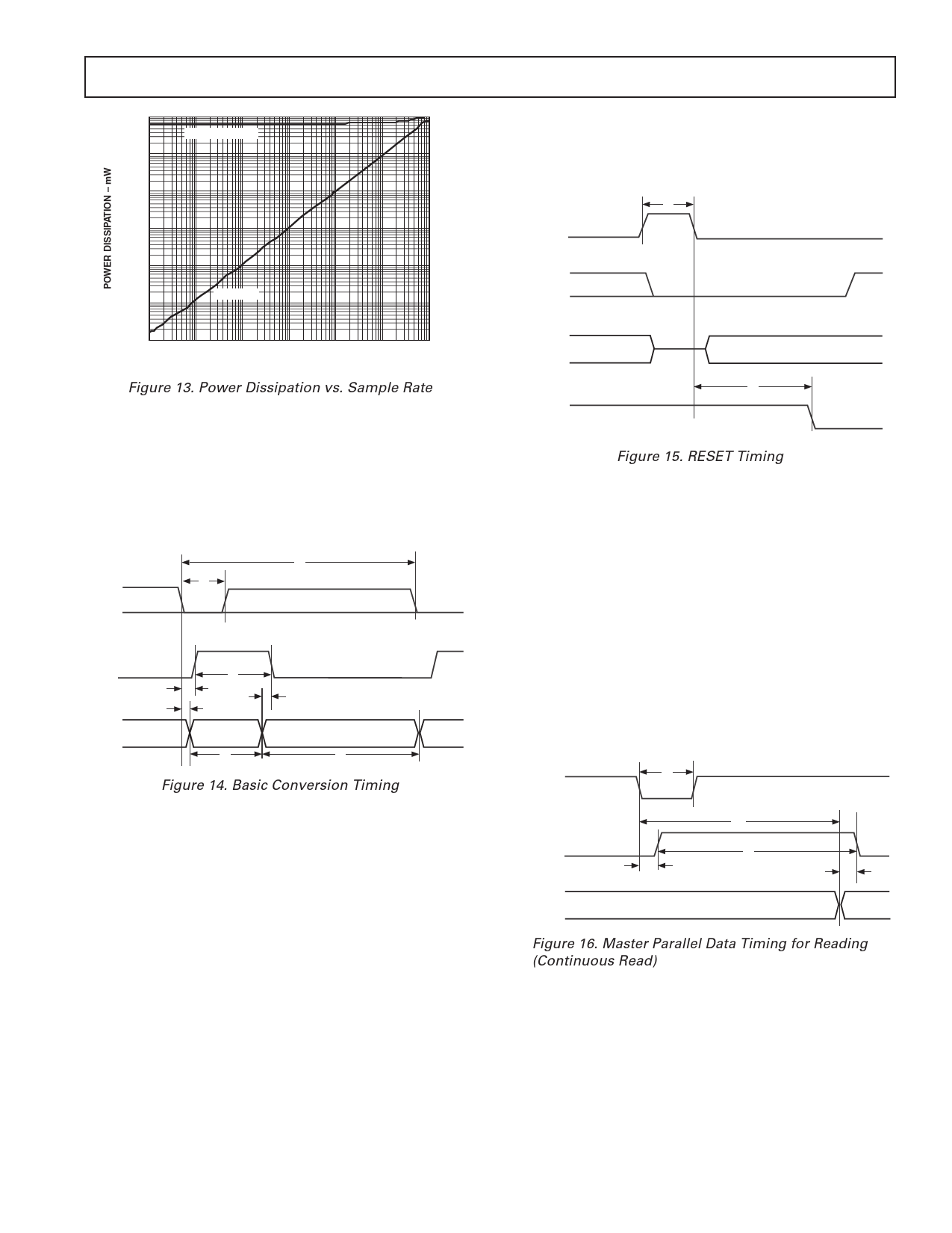
100000
10000
1000
100
WARP/NORMAL
AD15700
For applications where the SNR is critical, CNVST signal should
have a very low jitter. One way to achieve that is to use a dedicated
oscillator for CNVST generation, or at least to clock it with a
high frequency low jitter clock.
t9
RESET
10
IMPULSE
1
BUSY
0.1
1
10
100
1000 10000 100000 1000000
SAMPLING RATE – SPS
Figure 13. Power Dissipation vs. Sample Rate
CONVERSION CONTROL
Figure 14 shows the detailed timing diagrams of the conversion
process. The ADC is controlled by the signal CNVST, which
initiates conversion. Once initiated, it cannot be restarted or
aborted, even by the power-down input PD, until the conver-
sion is complete. The CNVST signal operates independently of
CS_ADC and RD signals.
t2
t1
CNVST
BUSY
t3
t5
MODE ACQUIRE
t4
CONVERT
t7
t6
ACQUIRE
t8
CONVERT
Figure 14. Basic Conversion Timing
In impulse mode, conversions can be automatically initiated.
If CNVST is held low when BUSY is low, the ADC controls the
acquisition phase and then automatically initiates a new conversion.
By keeping CNVST low, the ADC keeps the conversion process
running by itself. It should be noted that the analog input has to
be settled when BUSY goes low. Also, at power-up, CNVST
should be brought low once to initiate the conversion process.
In this mode, the ADC could sometimes run slightly faster than
the guaranteed limits in the impulse mode of 666 kSPS. This
feature does not exist in warp or normal modes.
Although CNVST is a digital signal, it should be designed with
special care with fast, clean edges, and levels with minimum
overshoot and undershoot or ringing. It is a good thing to shield
the CNVST trace with ground and also to add a low value serial
resistor (i.e., 50 W) termination close to the output of the com-
ponent that drives this line.
DATA
t8
CNVST
Figure 15. RESET Timing
DIGITAL INTERFACE
The ADC has a versatile digital interface; it can be interfaced with
the host system by using either a serial or parallel interface. The
serial interface is multiplexed on the parallel data bus. The ADC
digital interface also accommodates both 3 V or 5 V logic by simply
connecting the OVDD supply pin of the ADC to the host system
interface digital supply. Finally, by using the OB/2C input pin,
both straight binary or twos complement coding can be used.
The two signals, CS_ADC and RD, control the interface. When
at least one of these signals is high, the interface outputs are in
high impedance. Usually, CS_ADC allows the selection of each
ADC in multicircuit applications and is held low in a single
ADC design. RD is generally used to enable the conversion
result on the data bus.
CS_ADC = RD = 0
t1
CNVST
BUSY
DATA BUS
t10
t4
t3
PREVIOUS CONVERSION DATA
t11
NEW DATA
Figure 16. Master Parallel Data Timing for Reading
(Continuous Read)
REV. A
–31–
Share Link: 