4501GSD 查看數據表(PDF) - Advanced Power Electronics Corp
零件编号
产品描述 (功能)
生产厂家
4501GSD Datasheet PDF : 7 Pages
| |||
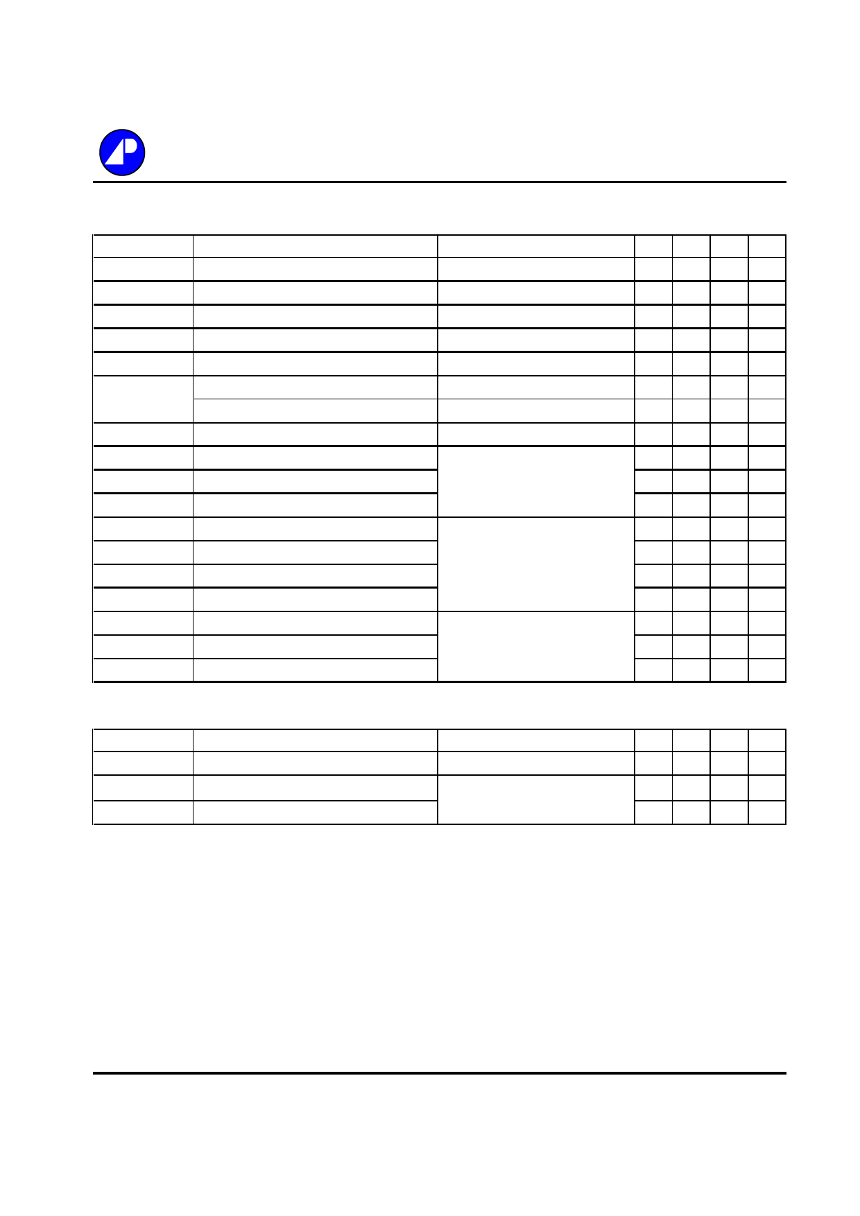
AP4501GSD
P-CH Electrical Characteristics@Tj=25oC(unless otherwise specified)
Symbol
Parameter
Test Conditions
Min. Typ. Max. Units
BVDSS
RDS(ON)
Drain-Source Breakdown Voltage
Static Drain-Source On-Resistance2
VGS=0V, ID=-250uA
VGS=-10V, ID=-5A
VGS=-4.5V, ID=-3A
-30 - - V
- - 49 mΩ
- - 75 mΩ
VGS(th)
Gate Threshold Voltage
VDS=VGS, ID=-250uA
-1 - -3 V
gfs
IDSS
IGSS
Qg
Qgs
Qgd
td(on)
tr
td(off)
tf
Ciss
Coss
Crss
Forward Transconductance
Drain-Source Leakage Current ( Tj =25oC)
Drain-Source Leakage Current ( Tj =70oC)
Gate-Source Leakage
Total Gate Charge2
Gate-Source Charge
Gate-Drain ("Miller") Charge
Turn-on Delay Time2
Rise Time
Turn-off Delay Time
Fall Time
Input Capacitance
Output Capacitance
Reverse Transfer Capacitance
VDS=-10V, ID=-5A
VDS=-30V, VGS=0V
VDS=-24V, VGS=0V
VGS=±20V
ID=-5A
VDS=-15V
VGS=-4.5V
VDS=-15V
ID=-1A
RG=3.3Ω,VGS=-10V
RD=15Ω
VGS=0V
VDS=-25V
f=1.0MHz
- 5 -S
- - -1 uA
- - -25 uA
- - ±100 nA
- 8 15 nC
- 1.7 - nC
- 4.5 - nC
- 6.7 - ns
- 10 - ns
- 21 - ns
- 10 - ns
- 595 730 pF
- 80 - pF
- 75 - pF
Source-Drain Diode
Symbol
VSD
trr
Parameter
Forward On Voltage2
Reverse Recovery Time2
Qrr
Reverse Recovery Charge
Test Conditions
IS=-1.7A, VGS=0V
IS=-5A, VGS=0V,
dI/dt=100A/µs
Min. Typ. Max. Units
- - -1.2 V
- 18 - ns
- 11 - nC
Notes:
1.Pulse width limited by Max. junction temperature.
2.Pulse test
3.Mounted on 1 in2 copper pad of FR4 board ; 90℃/W when mounted on Min. copper pad.
THIS PRODUCT IS AN ELECTROSTATIC SENSITIVE, PLEASE HANDLE WITH CAUTION.
THIS PRODUCT HAS BEEN QUALIFIED FOR CONSUMER MARKET. APPLICATIONS OR USES AS CRITERIAL COMPONENT IN LIFE SUPPORT
DEVICE OR SYSTEM ARE NOT AUTHORIZED.
3/7
Share Link: 