CXB1563Q 查看數據表(PDF) - Sony Semiconductor
零件编号
产品描述 (功能)
生产厂家
CXB1563Q Datasheet PDF : 16 Pages
| |||
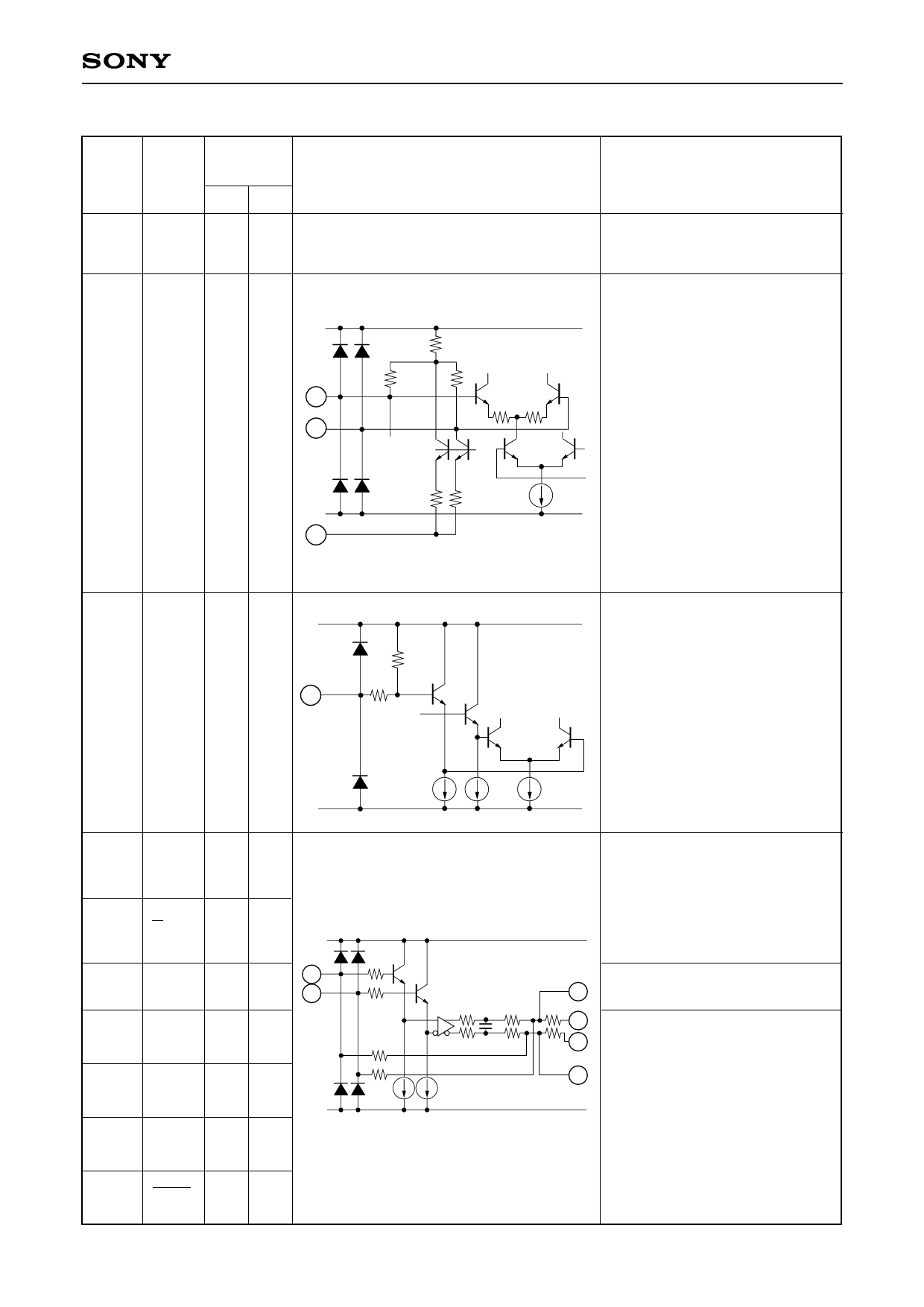
Pin Description
Typical pin
Pin No. Symbol voltage (V)
DC AC
1,2 VCCA 0V
31
3 VEEI –5V
30
3
CXB1563Q
Equivalent circuit
Description
Positive power supply for analog
block.
993
110.3
110.3
Vcs
VccA
SW
VEEA
Generates the default voltage
between UP and DOWN.
The voltage (8.0mV for input
conversion) can be generated
between UP and DOWN
(Pins 30 and 31) as alarm
setting level by connecting this
pin to VEEA.
0V
4
SW
(OPEN)
or
4
–5V
5D
–0.9V
–1.3V to
–1.7V
6D
–0.9V
–1.3V to
–1.7V
5
7
VCCA 0V
6
8 CAP1 –1.8V
9 R1K
10 R2K
11 CAP1 –1.8V
150k
100k
VREF
VCCA
Switches the identification
maximum voltage amplitude.
High voltage when open; the
identification maximum voltage
amplitude becomes 50mVp-p.
Low voltage when connecting
this pin to VEE; the amplitude
becomes 20mVp-p.
VEEA
Limiting amplifier block input.
Be sure to make this input with
AC coupled.
VCCA
200
Positive power supply for analog
11 block.
200
10k 100p 200 2k
10 Pins 8 and 11 connect a
1.5k
10k 200 1k 9 capacitor which determines the
cut-off frequency for feedback
8 block, and 1kΩ is connected
1.5k
VEEA between Pins 8 and 9; 2kΩ
between Pins 10 and 11. A
resistor which is to be inserted in
parallel with a capacitor can be
selected 5 ways by external
wiring, and DC feedback can be
varied.
–3–
Share Link: 