M30621MCM-F52GP 查看數據表(PDF) - MITSUBISHI ELECTRIC
零件编号
产品描述 (功能)
生产厂家
M30621MCM-F52GP Datasheet PDF : 237 Pages
| |||
Memory
Mitsubishi microcomputers
M16C / 62A Group (80-pin)
SINGLE-CHIP 16-BIT CMOS MICROCOMPUTER
Operation of Functional Blocks
The M16C/62A (80-pin version) group accommodates certain units in a single chip. These units include
ROM and RAM to store instructions and data and the central processing unit (CPU) to execute arithmetic/
logic operations. Also included are peripheral units such as timers, serial I/O, D-A converter, DMAC, CRC
calculation circuit, A-D converter, and I/O ports.
The following explains each unit.
Memory
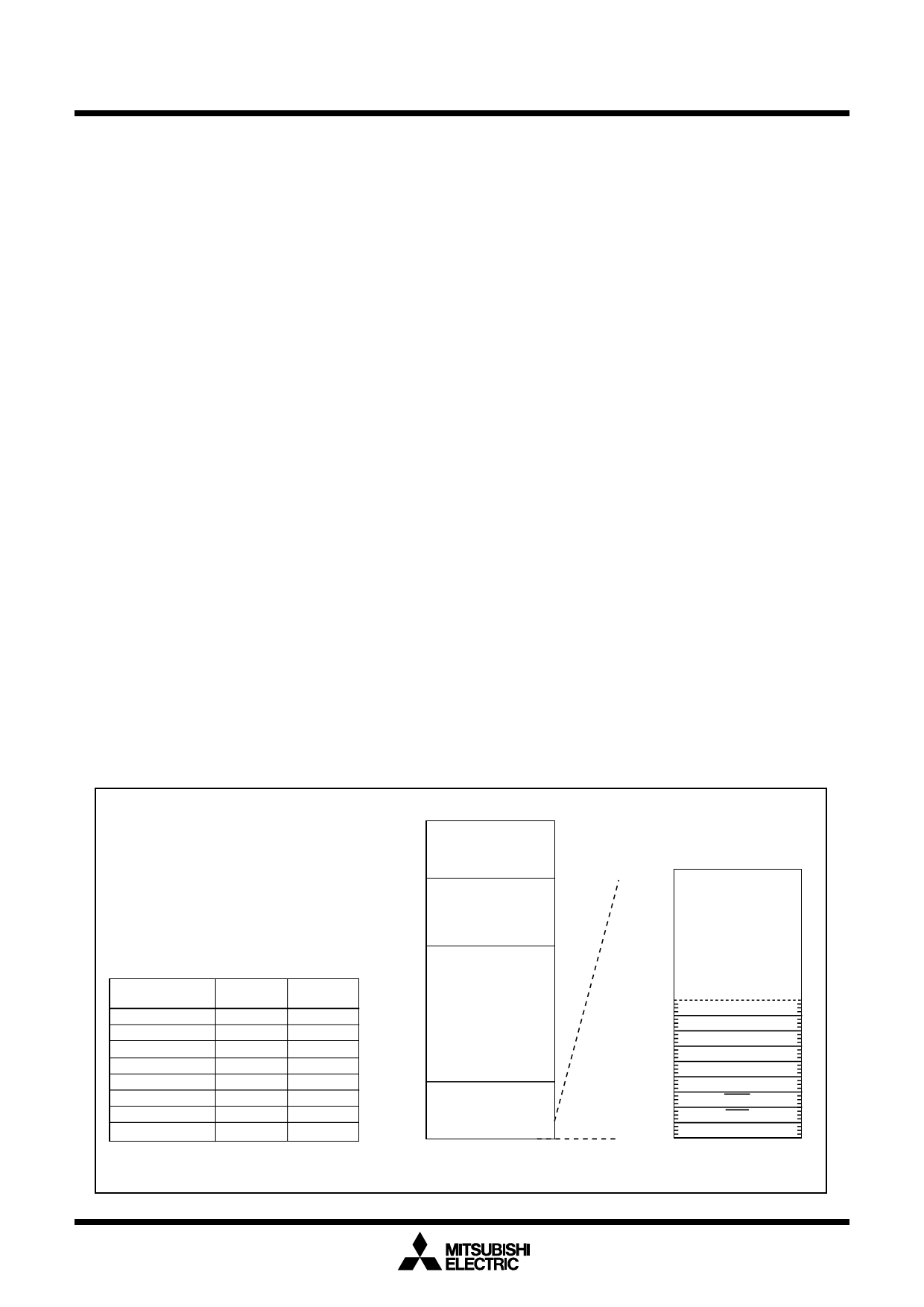
Figure 1.4.1 is a memory map of the M16C/62A (80-pin version) group. The address space extends the 1M
bytes from address 0000016 to FFFFF16. From FFFFF16 down is ROM. For example, in the M30623MCA-
XXXGP, there is 128K bytes of internal ROM from E000016 to FFFFF16. The vector table for fixed interrupts
_______
such as the reset and NMI are mapped to FFFDC16 to FFFFF16. The starting address of the interrupt
routine is stored here. The address of the vector table for timer interrupts, etc., can be set as desired using
the internal register (INTB). See the section on interrupts for details.
From 0040016 up is RAM. For example, in the M30623MCA-XXXGP, 5K bytes of internal RAM is mapped
to the space from 0040016 to 017FF16. In addition to storing data, the RAM also stores the stack used when
calling subroutines and when interrupts are generated.
The SFR area is mapped to 0000016 to 003FF16. This area accommodates the control registers for periph-
eral devices such as I/O ports, A-D converter, serial I/O, and timers, etc. Figures 1.7.1 to 1.7.3 are location
of peripheral unit control registers. Any part of the SFR area that is not occupied is reserved and cannot be
used for other purposes.
The special page vector table is mapped to FFE0016 to FFFDB16. If the starting addresses of subroutines
or the destination addresses of jumps are stored here, subroutine call instructions and jump instructions
can be used as 2-byte instructions, reducing the number of program steps.
0000016
SFR area
For details, see Figures
1.7.1 to 1.7.3
0040016
Internal RAM area
XXXXX16
FFE0016
Special page
vector table
Type No.
M30623M4A
M30623M8A
M30623MAA
M30623MCA
M30621M8A
M30621MCA/FCA
M30621MAA
M30625MGA/FGA
Address
XXXXX16
00FFF16
013FF16
017FF16
017FF16
02BFF16
02BFF16
02BFF16
053FF16
Address
YYYYY16
F800016
F000016
E800016
E000016
F000016
E000016
E800016
C000016
Reserved
area
YYYYY16
Internal ROM area
FFFFF16
FFFDC16
FFFFF16
Undefined instruction
Overflow
BRK instruction
Address match
Single step
Watchdog timer
DBC
NMI
Reset
Note: Set PM13 to “1” in M30625MGA/FGA. Otherwise set PM13 to “0”.
Figure 1.4.1. Memory map
10
Share Link: 