S504T 查看數據表(PDF) - Vishay Semiconductors
零件编号
产品描述 (功能)
生产厂家
S504T Datasheet PDF : 5 Pages
| |||
S504T/S504TR/S504TRW
Vishay Semiconductors
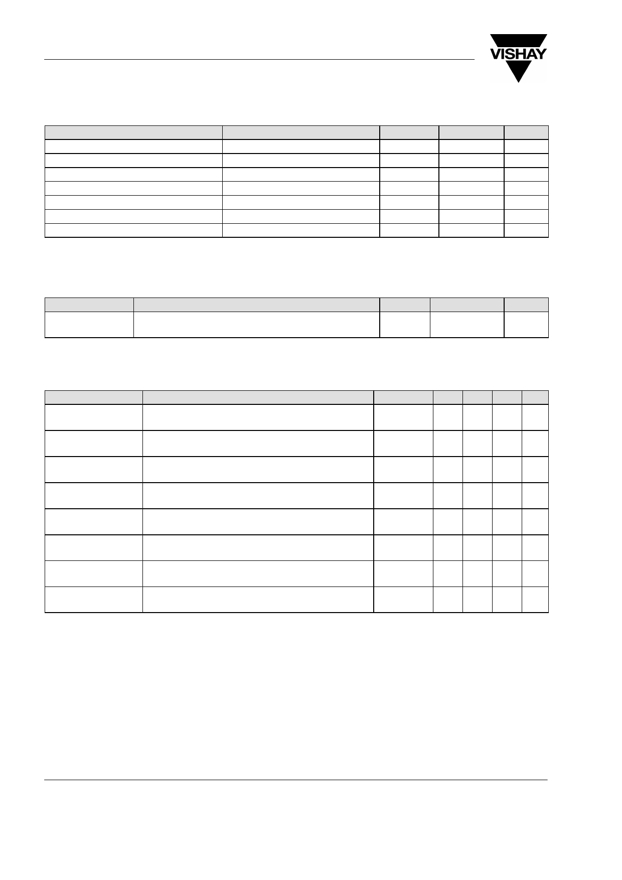
Absolute Maximum Ratings
Tamb = 25_C, unless otherwise specified
Parameter
Drain - source voltage
Drain current
Gate 1/Gate 2 - source peak current
Gate 1/Gate 2 - source voltage
Total power dissipation
Channel temperature
Storage temperature range
Test Conditions
Tamb ≤ 60 °C
Symbol
Value
Unit
VDS
8
V
ID
25
mA
±IG1/G2SM
10
mA
±VG1/G2SM
6
V
Ptot
200
mW
TCh
150
°C
Tstg
–55 to +150 °C
Maximum Thermal Resistance
Tamb = 25_C, unless otherwise specified
Parameter
Test Conditions
Symbol
Value
Unit
m Channel ambient on glass fibre printed board (25 x 20 x 1.5) mm3
plated with 35 m Cu
RthChA
450
K/W
Electrical DC Characteristics
Tamb = 25_C, unless otherwise specified
Parameter
Test Conditions
Drain - source
m ID = 10 A, VG1S = VG2S = 0
breakdown voltage
Gate 1 - source
±IG1S = 10 mA, VG2S = VDS = 0
breakdown voltage
Gate 2 - source
±IG2S = 10 mA, VG1S = VDS = 0
breakdown voltage
Gate 1 - source
leakage current
+VG1S = 5 V, VG2S = VDS = 0
Gate 2 - source
leakage current
Drain - source op-
erating current
Gate 1 - source
cut-off voltage
Gate 2 - source
cut-off voltage
±VG2S = 5 V, VG1S = VDS = 0
W VDS = VRG1 = 5 V, VG2S = 4 V, RG1 = 220 k
m VDS = 5 V, VG2S = 4 V, ID = 20 A
W m VDS = VRG1 = 5 V, RG1 = 220 k , ID = 20 A
Symbol Min Typ Max Unit
V(BR)DSS 15
V
±V(BR)G1SS 7
10 V
±V(BR)G2SS 7
10 V
+IG1SS
20 nA
±IG2SS
20 nA
IDSO
7 10 14 mA
VG1S(OFF) 0.4
1.2 V
VG2S(OFF)
1.0
V
Remark on driving the MOSMIC and improving intermodulation behavior:
W By setting RG1 = 150 k typical value of IDSO will raise up to 15 mA and improved intermodulation behavior will
be performed.
www.vishay.com
2 (5)
Document Number 85043
Rev. 5, 05-Jun-01
Share Link: 