AS1712 وں¥çœ‹و•¸و“ڑè،¨ï¼ˆPDF) - austriamicrosystems AG
零ن»¶ç¼–هڈ·
ن؛§ه“پوڈڈè؟° (هٹں能)
ç”ںن؛§هژ‚ه®¶
AS1712
austriamicrosystems AG

AS1712 Datasheet PDF : 17 Pages
| |||
AS1710/AS1712
Data Sheet - Application Information
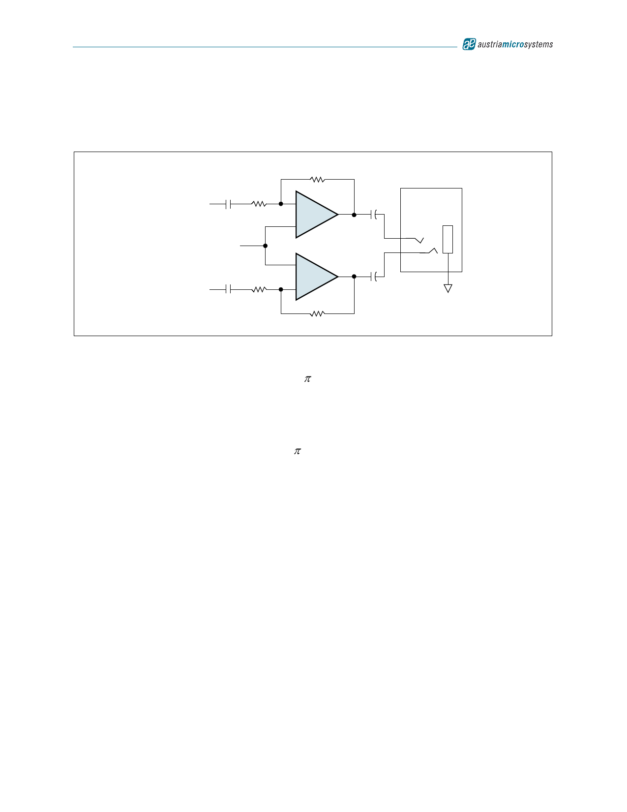
60mW Single-Supply Stereo Headphone Driver
Two AS1710 amplifiers can be used as a single-supply, stereo headphone driver. The circuit shown in Figure 22 can
deliver 60mW per channel with 1% distortion from a single 5V supply.
Figure 22. Stereo Headphone Driver Application (with Coupling Capacitor)
RF
Audio In CIN
RIN
Left
VBIAS
Audio In
Right
CIN
RIN
–
AS1710
+
+
AS1710
–
COUT
+
Headphone Jack
to 32خ© Stereo
Headset
COUT
+
RF
In Figure 22, CIN and RIN form a high-pass filter that removes the DC bias from the incoming signal. The -3dB point of
the high-pass filter is given by:
f-3dB = 1/(2د€RINCIN)
(EQ 4)
Choose gain-setting resistors RIN and RF according to the amount of desired gain, keeping in mind the maximum out-
put amplitude.
COUT blocks the DC component of the amplifier output, preventing DC current flowing to the load. The output capacitor
and the load impedance form a high-pass filter with the -3dB point determined by:
f-3dB = 1/(2د€RLOADCOUT)
(EQ 5)
For a 32خ© load, a 100آµF aluminum electrolytic capacitor gives a low-frequency pole at 50Hz.
Rail-to-Rail Input Stage
The AS1710/AS1712 CMOS op amps have parallel connected N- and P-channel differential input stages that combine
to accept a common-mode range extending to both supply rails. The N-channel stage is active for common-mode input
voltages typically greater than (VSS + 1.2V), and the p-channel stage is active for common-mode input voltages typi-
cally less than (VDD - 1.2V).
Rail-to-Rail Output Stage
The minimum output is within millivolts of ground for single- supply operation, where the load is referenced to ground
(VSS). Figure 23 shows the input voltage range and the output voltage swing of an AS1710 connected as a voltage fol-
lower. The maximum output voltage swing is load dependent although it is guaranteed to be within 500mV of the posi-
tive rail (VDD = 2.7V) even with maximum load (32خ© to ground).
www.austriamicrosystems.com
Revision 1.04
10 - 17
Share Link: