AS1746-BTDR 查看數據表(PDF) - austriamicrosystems AG
零件编号
产品描述 (功能)
生产厂家
AS1746-BTDR Datasheet PDF : 15 Pages
| |||
AS1746
Datasheet - Application Information
9 Application Information
Digital Control Inputs
The AS1746 logic inputs can handle up to +5.5V regardless of the supply voltage. For example, with a +3.3V supply,
INx may be driven low to GND and high to 5.5V. Driving INx rail-to-rail minimizes power consumption.
Analog Signal Levels
Analog signals that range over the entire supply voltage (V+ to GND) are passed with very little change in RON (see
Typical Operating Characteristics on page 6). The switches are bi-directional, so the NOx, NCx, and COMx pins can be
used as inputs or outputs.
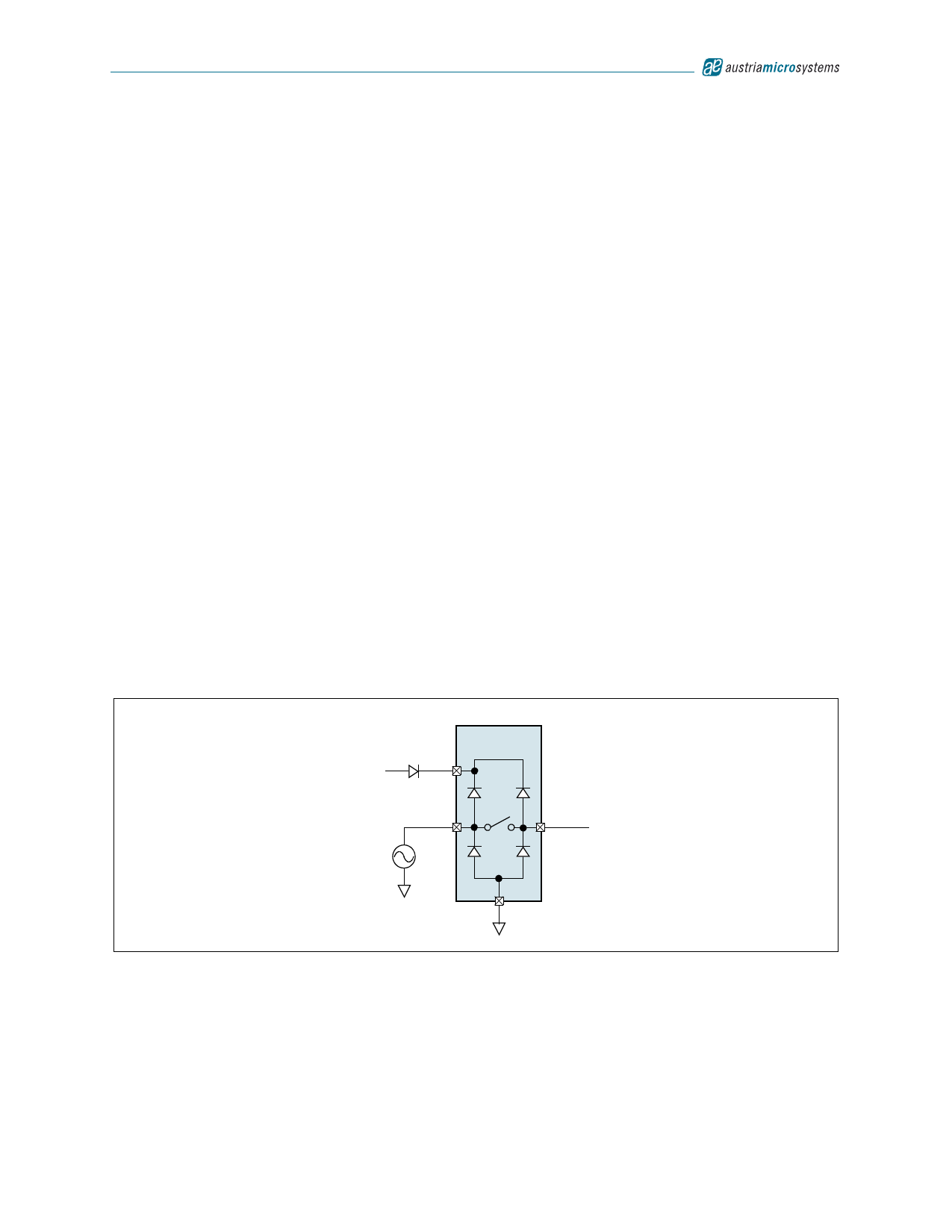
Power Supply Sequencing
Proper power supply sequencing is recommended for all CMOS devices. The recommended sequence is as follows:
1. V+
2. NOx, NCx, COMx
Always apply V+ before applying analog signals, especially if the analog signal is not current limited. If this sequencing
is not possible, and if the analog inputs are not current limited to <20mA, add a small signal protection diode (D1) as
shown in Figure 16.
Overvoltage Protection
Using a protection diode will reduce the analog range to a diode voltage drop (approximately 0.7V) below V+ (for D1).
RON will increase slightly at low supply voltages.
Caution: The maximum supply voltage (V+) must not exceed +7V. Do not exceed the absolute maximum ratings
because stresses beyond the ratings listed in Absolute Maximum Ratings on page 3 may cause permanent
damage to the device.
Note: Protection diode D1 can also protect the device from some overvoltage conditions.
Figure 16. Overvoltage Protections using 2 External Blocking Diodes
Positive
Supply
D1 V+
AS1746
NO
VGEN
COM
GND
Note: No damage will result to the circuit shown in Figure 16 if the supply voltage is below the absolute maximum rat-
ing applied to an analog signal pin (NOx, NCx, or COMx).
www.austriamicrosystems.com
Revision 1.03
9 - 15
Share Link: 