M66008FP 查看數據表(PDF) - Mitsumi
零件编号
产品描述 (功能)
生产厂家
M66008FP Datasheet PDF : 5 Pages
| |||
MITSUBISHI 〈DIGITAL ASSP〉
M66008P/FP
16-BIT I/O EXPANDER
FUNCTION
The M66008 uses a silicon gate CMOS process to achieve
low power consumption and high noise margin.
The M66008 independently forms a 16-bit serial input-paral-
lel output shift register and a parallel input-serial output shift
register to read serial input data during output of serial data
converted from parallel data.
The operation for serial output of 16-bit parallel data and op-
eration for reading serial data from MCU by changing CS
from “H” to “L”. That is, at a falling edge of CS, 16-bit parallel
data is latched and serial data is output from the DO pin in
synchronization with 16-bit parallel data at a falling edge of
shift clock. In addition, serial data from MCU is read into an
internal shift register via the DI pin at a rising edge of shift
clock. The 17th bit shift clock and later clocks are ignored.
When the reading operation is masked, the DO pin is placed
in high impedance status. When CS changes from “L” to “H”,
16-bit serial data read from the DI pin is output to pins D1 to
D16 in parallel.
Since the output format of the parallel output pin is set to N-
channel open drain output, write “H” data into a terminal
placed in input mode.
OPERATION DESCRIPTION
(1) When power is turned on, DO and D1~D16 are indetermi-
nate. However, they are placed in high impedance status
by setting S to “L”.
(2) The status of D1 to D16 is loaded to shift register ! at a
falling edge of CS.
(3) At a falling edge of CLK, 16-bit serial output of the data
loaded in step (2) is sequentially performed from DO.
(4) At a rising edge of CLK, 16-bit serial data is written into
shift register @ from DI.
(5) CLK of 17th bit and later is ignored and serial data cannot
be written. DO is placed in high impedance status.
(6) At a rising edge of CS, data written in step (4) is output to
D1 to D16.
(7) Shift register ! loads data to be applied externally and
AND data having the latched content to parallel output
latch.
(8) When CS is activated before arrival of CLK at the 16th bit,
parallel output latch outputs to D1 to D16 by latching the
data that has been written into shift register @. Shift reg-
isters ! and @ continues the shift operation until it arrives
at the 16th bit of CLK and DO output serial data.
(9) Serial data is used to control the operation for switching
input/output mode of D1 to D16. The pin set to “H” oper-
ates as an input pin.
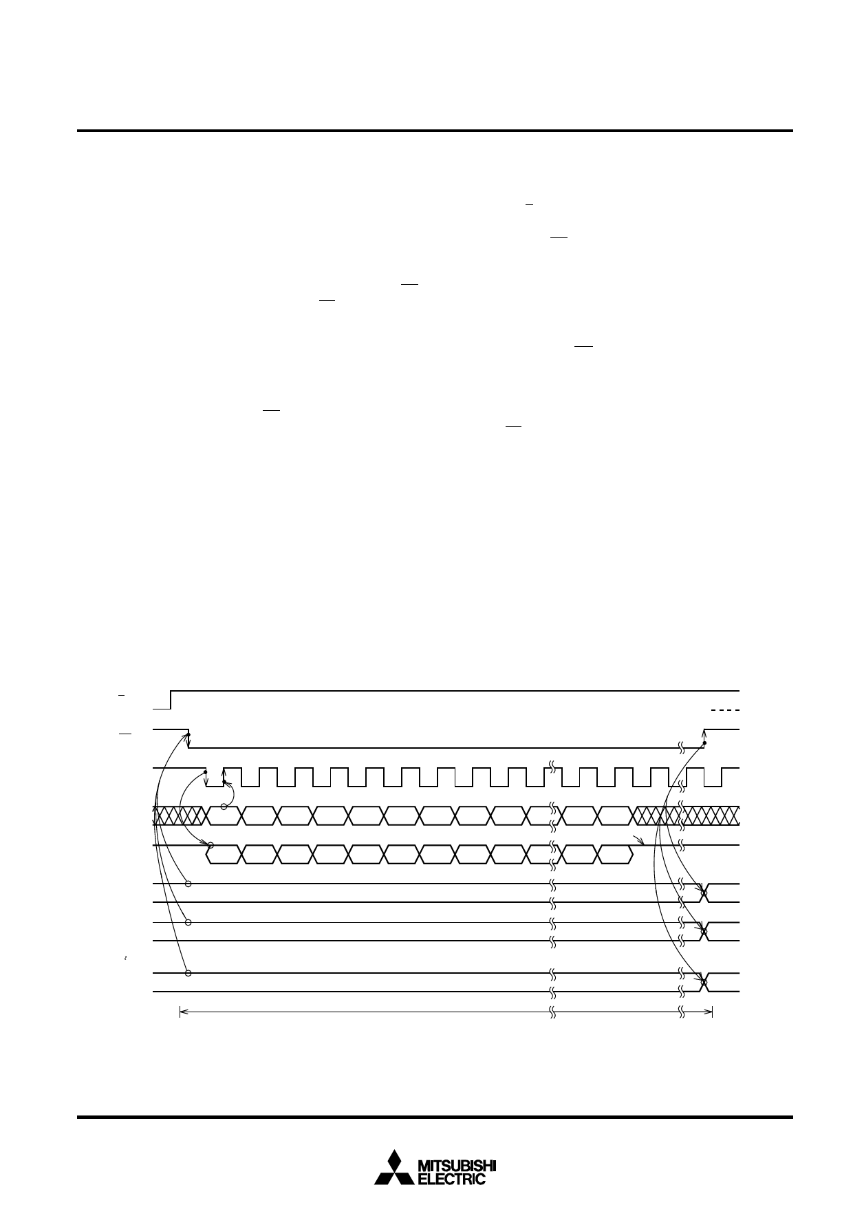
OPERATION TIMING DIAGRAM
S
(1)
CS
(2)
(5)
CLK
1
2
3
4
5
6
7
8
9
10 15 16 17
(4)
DI
DO1 DO2 DO3 DO4 DO5 DO6 DO7 DO8 DO9
DO15 DO16
(3)
High impedance
DO
DI1 DI2 DI3 DI4 DI5 DI6 DI7 DI8 DI9
DI15 DI16
D1
DI1
D2
DI2
DI6
DI16
1 cycle
H
L
(6)
DO1
DO2
DO16
2
Share Link: 