W77C32-25 查看數據表(PDF) - Winbond
零件编号
产品描述 (功能)
生产厂家
W77C32-25 Datasheet PDF : 71 Pages
| |||

Preliminary W77C32
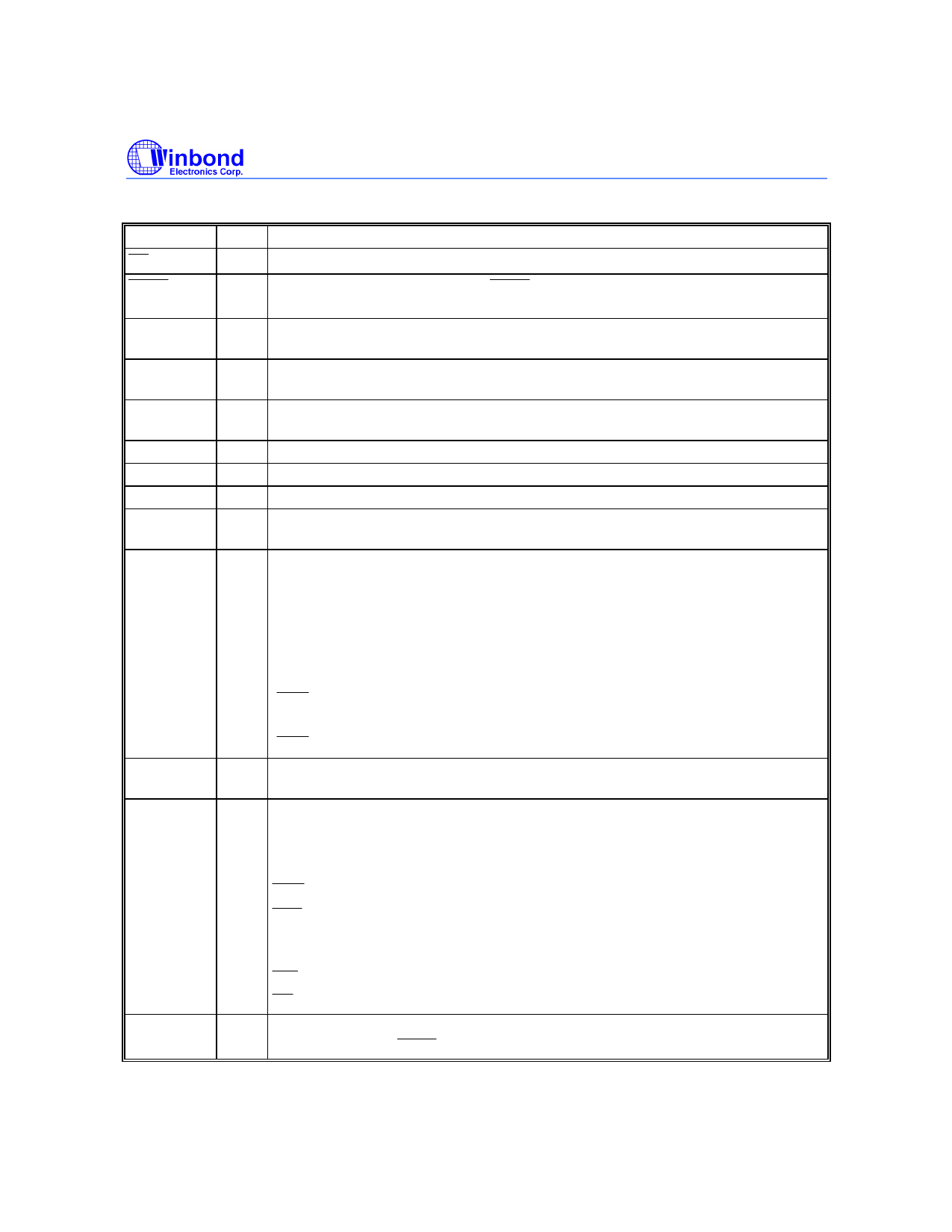
PIN DESCRIPTION
SYMBOL
EA
PSEN
ALE
RST
XTAL1
XTAL2
VSS
VDD
P0.0−P0.7
P1.0−P1.7
P2.0−P2.7
P3.0−P3.7
TYPE
DESCRIPTIONS
I EXTERNAL ACCESS ENABLE: It should be kept low.
O PROGRAM STORE ENABLE: PSEN enables the external ROM data onto the
Port 0 address/data bus during fetch and MOVC operations.
O ADDRESS LATCH ENABLE: ALE is used to enable the address latch that
separates the address from the data on Port 0.
I RESET: A high on this pin for two machine cycles while the oscillator is running
resets the device.
I CRYSTAL1: This is the crystal oscillator input. This pin may be driven by an
external clock.
O CRYSTAL2: This is the crystal oscillator output. It is the inversion of XTAL1.
I GROUND: Ground potential
I POWER SUPPLY: Supply voltage for operation.
I/O PORT 0: Port 0 is an open-drain bi-directional I/O port. This port also provides a
multiplexed low order address/data bus during accesses to external memory.
I/O PORT 1: Port 1 is a bi-directional I/O port with internal pull-ups. The bits have
alternate functions which are described below:
T2(P1.0): Timer/Counter 2 external count input
T2EX(P1.1): Timer/Counter 2 Reload/Capture/Direction control
RXD1(P1.2): Serial port 1 RXD
TXD1(P1.3): Serial port 1 TXD
INT2(P1.4): External Interrupt 2
INT3 (P1.5): External Interrupt 3
INT4(P1.6): External Interrupt 4
INT5 (P1.7): External Interrupt 5
I/O PORT 2: Port 2 is a bi-directional I/O port with internal pull-ups. This port also
provides the upper address bits for accesses to external memory.
I/O PORT 3: Port 3 is a bi-directional I/O port with internal pull-ups. All bits have
alternate functions, which are described below:
RXD(P3.0) : Serial Port 0 input
TXD(P3.1) : Serial Port 0 output
INT0 (P3.2) : External Interrupt 0
INT1(P3.3) : External Interrupt 1
T0(P3.4) : Timer 0 External Input
T1(P3.5) : Timer 1 External Input
WR (P3.6) : External Data Memory Write Strobe
RD (P3.7) : External Data Memory Read Strobe
P4.0−P4.3
I/O PORT 4: Port 4 is a 4-bit bi-directional I/O port. The P4.0 also provides the
alternate function WAIT which is the wait state control signal.
* Note: TYPE I: input, O: output, I/O: bi-directional.
Publication Release Date: March 1999
-3-
Revision A1