BR93LC46 查看數據表(PDF) - ROHM Semiconductor
零件编号
产品描述 (功能)
生产厂家
BR93LC46 Datasheet PDF : 12 Pages
| |||
Memory ICs
BR93LC46 / BR93LC46F / BR93LC46RF / BR93LC46FV
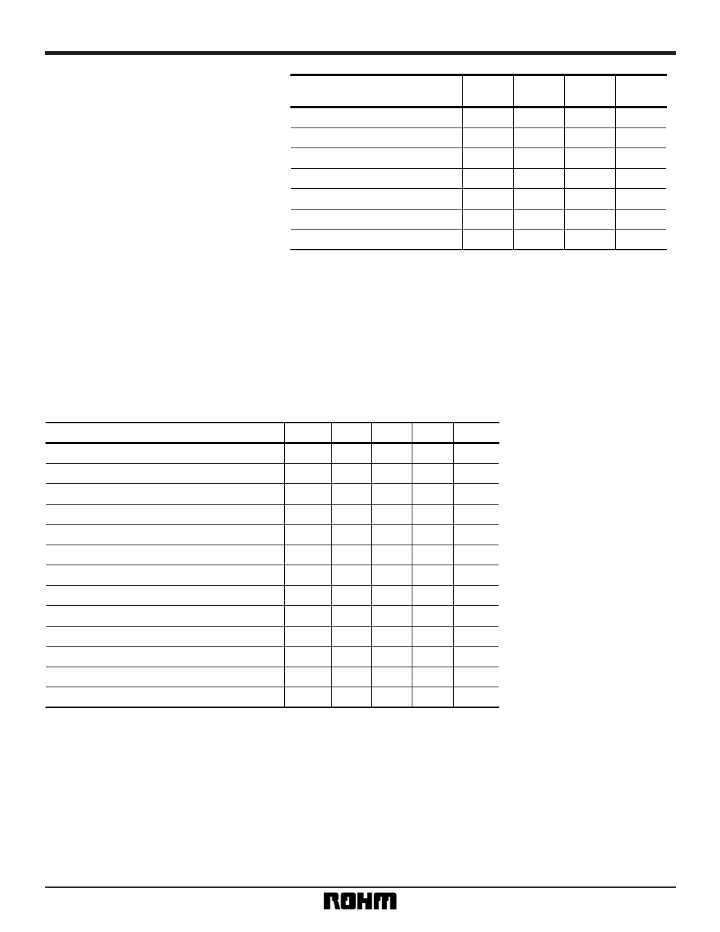
•Circuit operation
(1) Command mode
With these ICs, commands are not
recognized or acted upon until the
start bit is received. The start bit is
taken as the first “1” that is received
after the CS pin rises.
Command
Read (READ)∗1
Write enabled (WEN)
Write (WRITE)∗2
Write all addresses (WRAL)∗2
Start
bit
1
1
1
1
Operating Address
code
10 A5 ~ A0
Data
—
00 11XXXX —
01 A5 ~ A0 D15 ~ D0
00 01XXXX D15 ~ D0
∗1 After setting of the read command
Write disabled (WDS)
1
00 00XXXX —
and input of the SK clock, data corre-
sponding to the specified address is
output, with data corresponding to up-
per addresses then output in se-
Erase (ERASE)∗3
Chip erase (ERAL)∗3
X: Either VIH or VIL
1
11 A5 ~ A0 —
1
00 10XXXX —
quence. (Auto increment function)
∗2 When the write or write all addresses command is executed, all data in the selected memory cell is erased auto-
matically, and the input data is written to the cell.
∗3 These modes are optional modes. Please contact Rohm for information on operation timing.
(2) Operation timing characteristics
For 5V operation (unless otherwise noted, Ta = – 40 to + 85°C, VCC = 5V ± 10%)
Parameter
SK clock frequency
SK "H" time
SK "L" time
CS "L" time
CS setup time
DI setup time
CS hold time
DI hold time
Data "1" output delay time
Data "0" output delay time
Time from CS to output confirmation
Time from CS to output High impedance
Write cycle time
Symbol
fSK
tSKH
tSKL
tCS
tCSS
tDIS
tCSH
tDIH
tPD1
tPD0
tSV
tDF
tE / W
Min.
—
450
450
450
50
100
0
100
—
—
—
—
—
Typ.
—
—
—
—
—
—
—
—
—
—
—
—
—
Max.
1
—
—
—
—
—
—
—
500
500
500
100
10
Unit
MHz
ns
ns
ns
ns
ns
ns
ns
ns
ns
ns
ns
ms
4
Share Link: 