MC3411A 查看數據表(PDF) - Unspecified
零件编号
产品描述 (功能)
生产厂家
MC3411A Datasheet PDF : 29 Pages
| |||
MC3401A/3411A
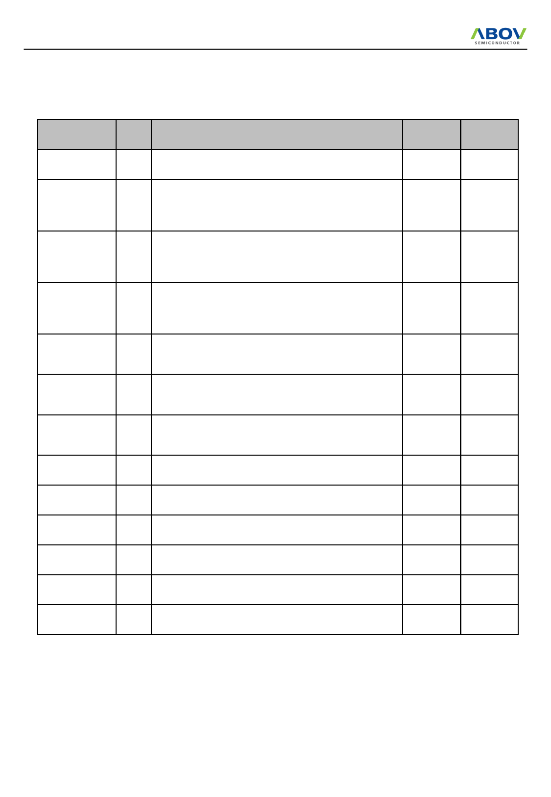
PIN DESCRIPTION
PIN NAME
LED1 to LED4
OSC
DOUT
DIN
(Schmitt
Trigger)
CLK
(Schmitt
Trigger)
STB
(Schmitt
Trigger)
K1 to K2
VSS
I/O
DESCRIPTION
PIN No.
(MC3401A)
O LED Output Pin
1 to 4
Oscillator Input Pin
I
A resistor is connected to this pin to determine the
oscillation
Frequency.
Data Output Pin (N-Channel, Open-Drain)
O
This pin outputs serial data at the falling edge of the shift
clock
(starting from the lower bit)
Data Input Pin
I
This pin inputs serial data at the rising edge of the shift
clock
(starting from the lower bit)
Clock Input Pin
I This pin reads serial data at the rising edge and outputs
data at the falling edge of the shift clock
Serial Interface Strobe Pin
I The data input after the STB has fallen is processed as a
command. When this in is “HIGH”, CLK is ignored.
Key Data Input Pins
I The data inputted to these pins is latched at the end of the
display cycle.
5
6
7
8
9
10, 11
- Logic Ground Pin
12, 44
PIN No.
(MC3411A)
1 to 4
5
7
8
9
10
11, 12
13, 48
VDD
- Logic Power Pin
SG1/KS1 to
SG16/KS16
O
High-Voltage Segment Output Pins
Also acts as the Key Source.
VEE
- Pull-Down Level
SG17/GR12 to
SG24/GR5
O
High-Voltage Segment/Grid Output Pins
GR4 to GR1
O High-Voltage Grid Output Pins
13, 43
14, 47
14 to 29
15 to 32
30
33
31 to 38
34 to 41
39 to 42
43 to 46
February 28, 2013 Ver. 1.10
6/29
Share Link: 