NCP1010(2010) 查看數據表(PDF) - ON Semiconductor
零件编号
产品描述 (功能)
生产厂家
NCP1010
(Rev.:2010)
(Rev.:2010)
ON Semiconductor

NCP1010 Datasheet PDF : 24 Pages
| |||
NCP1010, NCP1011, NCP1012, NCP1013, NCP1014
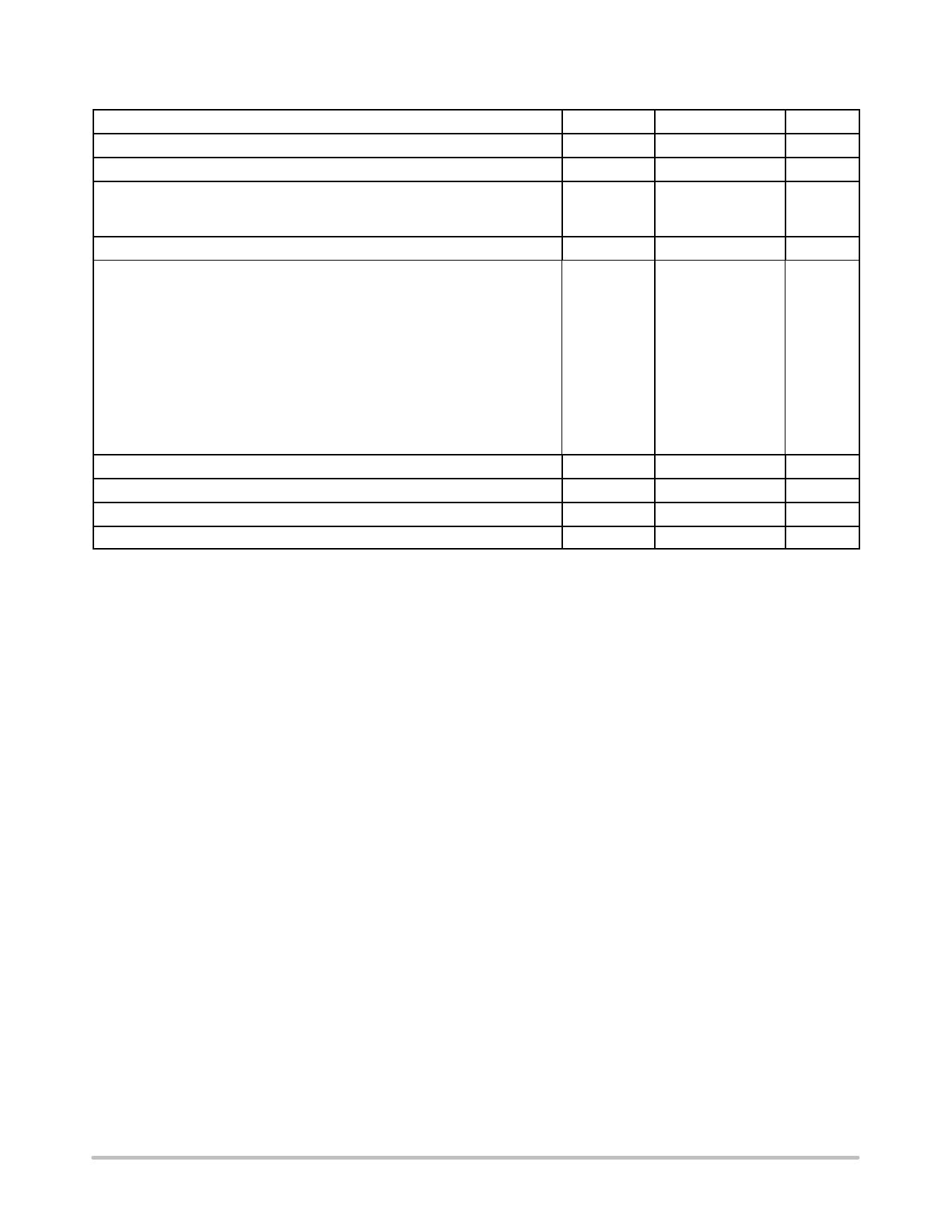
MAXIMUM RATINGS
Rating
Symbol
Value
Unit
Power Supply Voltage on all pins, except Pin 5 (Drain)
Drain Voltage
VCC
--0.3 to 10
V
--
--0.3 to 700
V
Drain Current Peak during Transformer Saturation
IDS(pk)
NCP1010/11
550
mA
NCP1012/13/14
1.0
A
Maximum Current into Pin 1 when Activating the 8.7 V Active Clamp
Thermal Characteristics
P Suffix, Case 626A
Junction--to--Lead
Junction--to--Air, 2.0 oz (70 mm) Printed Circuit Copper Clad
0.36 Sq. Inch (2.32 Sq. Cm)
1.0 Sq. Inch (6.45 Sq. Cm)
PL Suffix (Gull Wing), Case 626AA
Junction--to--Lead
Junction--to--Air, 2.0 oz (70 mm) Printed Circuit Copper Clad
0.36 Sq. Inch (2.32 Sq. Cm)
1.0 Sq. Inch (6.45 Sq. Cm)
ST Suffix, Plastic Package Case 318E
Junction--to--Lead
Junction--to--Air, 2.0 oz (70 mm) Printed Circuit Copper Clad
0.36 Sq. Inch (2.32 Sq. Cm)
1.0 Sq. Inch (6.45 Sq. Cm)
I_VCC
RθJL
RθJA
RθJL
RθJA
RθJL
RθJA
15
mA
C/W
9.0
77
60
11.9
92
71
14
74
55
Maximum Junction Temperature
Storage Temperature Range
TJmax
150
C
--
--60 to +150
C
ESD Capability, Human Body Model (All pins except HV)
--
2.0
kV
ESD Capability, Machine Model
--
200
V
Stresses exceeding Maximum Ratings may damage the device. Maximum Ratings are stress ratings only. Functional operation above the
Recommended Operating Conditions is not implied. Extended exposure to stresses above the Recommended Operating Conditions may affect
device reliability.
http://onsemi.com
4
Share Link: