AD790SQ/883 查看數據表(PDF) - Analog Devices
零件编号
产品描述 (功能)
生产厂家
AD790SQ/883 Datasheet PDF : 12 Pages
| |||
AD790
ABSOLUTE MAXIMUM RATINGS1, 2
Supply Voltage . . . . . . . . . . . . . . . . . . . . . . . . . . . . . . . . ± 18 V
Internal Power Dissipation2 . . . . . . . . . . . . . . . . . . . 500 mW
Differential Input Voltage . . . . . . . . . . . . . . . . . . . . . ± 16.5 V
Output Short-Circuit Duration . . . . . . . . . . . . . . . . Indefinite
Storage Temperature Range
(N, R) . . . . . . . . . . . . . . . . . . . . . . . . . . . –65°C to +125°C
(Q) . . . . . . . . . . . . . . . . . . . . . . . . . . . . . . –65°C to +150°C
Lead Temperature Range (Soldering 60 sec) . . . . . . . . 300°C
Logic Supply Voltage . . . . . . . . . . . . . . . . . . . . . . . . . . . . . 7 V
NOTES
1Stresses above those listed under “Absolute Maximum Ratings” may cause perma-
nent damage to the device. This is a stress rating only and functional operation of
the device at these or any other conditions above those indicated in the operational
sections of this specification is not implied. Exposure to absolute maximum rating
conditions for extended periods may affect device reliability.
2Thermal characteristics: plastic N-8 package: θJA = 90°C/watt; ceramic Q-8
package: θJA = 110°C/watt, θJC = 30°C/watt. SOIC (R-8) package: θJA = 160°C
watt; θJC = 42°C/watt.
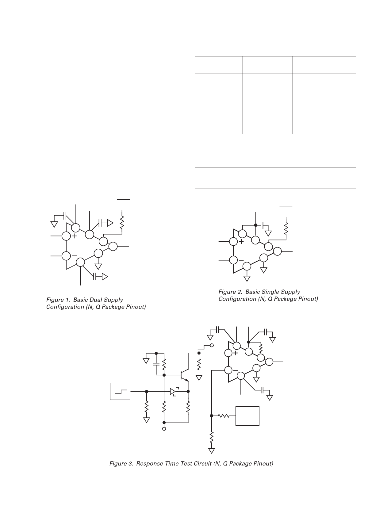
+ 15V
0.1µF
+ 5V
LATCH
(OPTIONAL)
0.1µF
510 Ω
1
+IN
2
8
5
AD790
7
OUTPUT
–IN
3
6
4
ORDERING GUIDE
Model
Temperature
Range
Package Package
Description Option
AD790JN
0°C to 70°C
AD790JR
0°C to 70°C
AD790JR-REEL 0°C to 70°C
AD790JR-REEL7 0°C to 70°C
AD790KN*
0°C to 70°C
AD790AQ
–40°C to +85°C
AD790BQ*
–40°C to +85°C
AD790SQ
–55°C to +125°C
Plastic DIP
SOIC
Reel
SOIC
Plastic DIP
Cerdip
Cerdip
Cerdip
N-8
SO-8
R-8
N-8
Q-8
Q-8
Q-8
*Not for new designs; obsolete April 2002.
For military processed devices, please refer to the standard Mi-
crocircuit Drawing (SMD) available at
www.dscc.dla.mil/programs/milspec/default.asp
SMD Part Number
ADI Equivalent
5962-9150501MPA*
*Not for new designs; obsolete April 2002.
AD790 SQ/883
+ 5V
0.1µF
LATCH
(OPTIONAL)
510Ω
1
+IN
2
8
5
AD790
7
OUTPUT
6
–IN
3
4
0.1µF
– 15V
Figure 1. Basic Dual Supply
Configuration (N, Q Package Pinout)
Figure 2. Basic Single Supply
Configuration (N, Q Package Pinout)
0.1µF
+15V +5V 0.1µF
PULSE
GENERATOR
–1.3V
–1.7V
HP8112
0.1µF
–100mV
130Ω
25Ω
1
2
8
AD790
3
4
1k
5
7
6
MPS
571
0.1µF
HP2835
50Ω 400Ω
650Ω
–5mV
–5V
–15V
10kΩ
–5V
VOLTAGE
SOURCE
10Ω
TEK
7904
SCOPE
Figure 3. Response Time Test Circuit (N, Q Package Pinout)
–4–
REV. D
Share Link: 