NX25F011A 查看數據表(PDF) - NexFlash -> Winbond Electronics
零件编号
产品描述 (功能)
生产厂家
NX25F011A
NexFlash -> Winbond Electronics

NX25F011A Datasheet PDF : 26 Pages
| |||
NX25F011A
NX25F041A
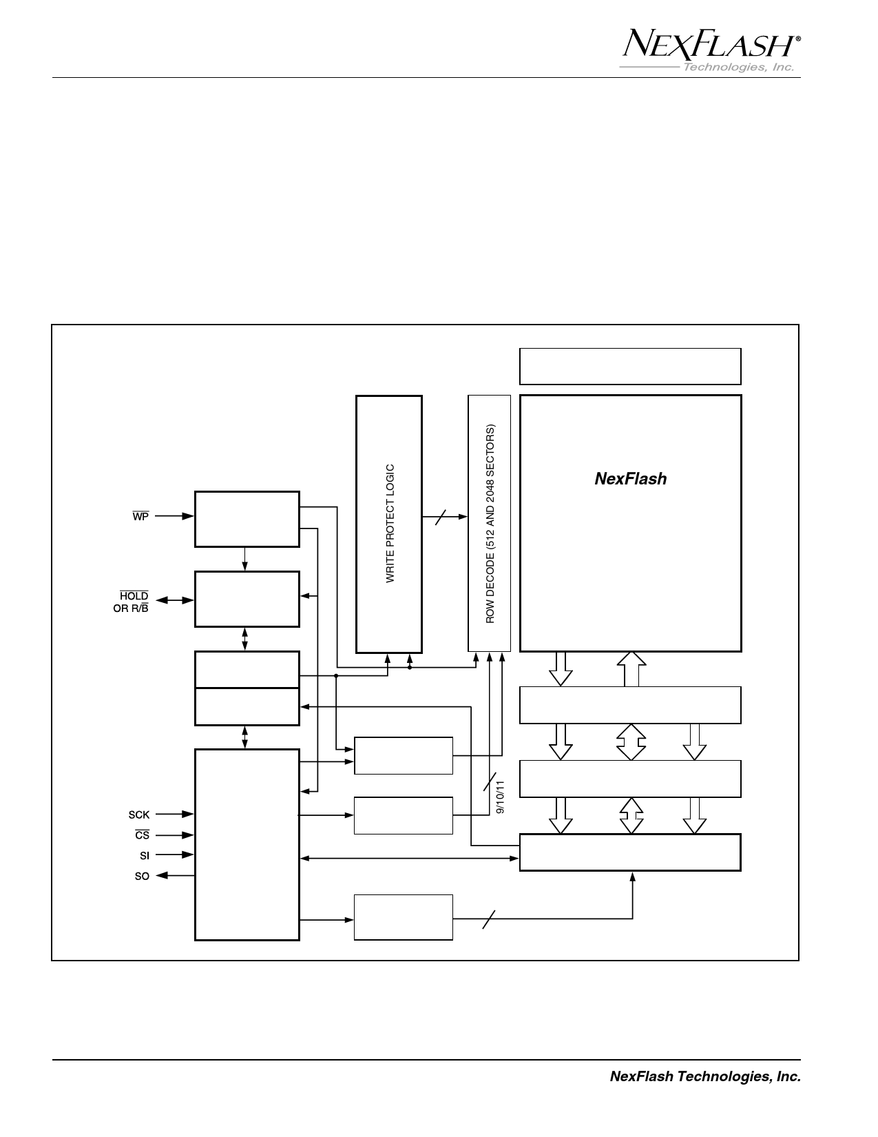
FUNCTIONAL OVERVIEW
An architectural block diagram of the NX25F011A and
NX25F041A is shown in Figure 2. Key elements of the
architecture include:
• SPI Interface and Command Set Logic
• Serial Flash Memory Array
• Serial SRAM and Program Buffer
• Write Protection Logic
• Configuration and Status Registers
• Device Information Sector
DEVICE INFORMATION SECTOR
(READ ONLY)
WRITE CONTROL
LOGIC
HOLD OR
READ/BUSY
LOGIC
NexFlash
1 AND 4 MEGABIT
16
SERIAL FLASH MEMORY ARRAY
512 AND 2048 BYTE-ADDRESSABLE
SECTORS OF 264 BYTES EACH
CONFIGURATION
REGISTER
STATUS
REGISTER
SPI
COMMAND
AND
CONTROL
LOGIC
HIGH-VOLTAGE
GENERATORS
SECTOR-ADDRESS
LATCH
DATA
BYTE-ADDRESS
LATCH/COUNTER
2112
PROGRAM BUFFER
(264 BYTES)
2112
SRAM
(264 BYTES)
8
8
8
COLUMN DECODE, SENSE AMP LATCH
AND DATA COMPARE LOGIC
9
Figure 2. NX25F011A and NX25F041A Architectural Block Diagram
2
NexFlash Technologies, Inc.
PRELIMINARY NXSF014B-0699
06/11/99
Share Link: