NX25F011A 查看數據表(PDF) - NexFlash -> Winbond Electronics
零件编号
产品描述 (功能)
生产厂家
NX25F011A
NexFlash -> Winbond Electronics

NX25F011A Datasheet PDF : 26 Pages
| |||
NX25F011A
NX25F041A
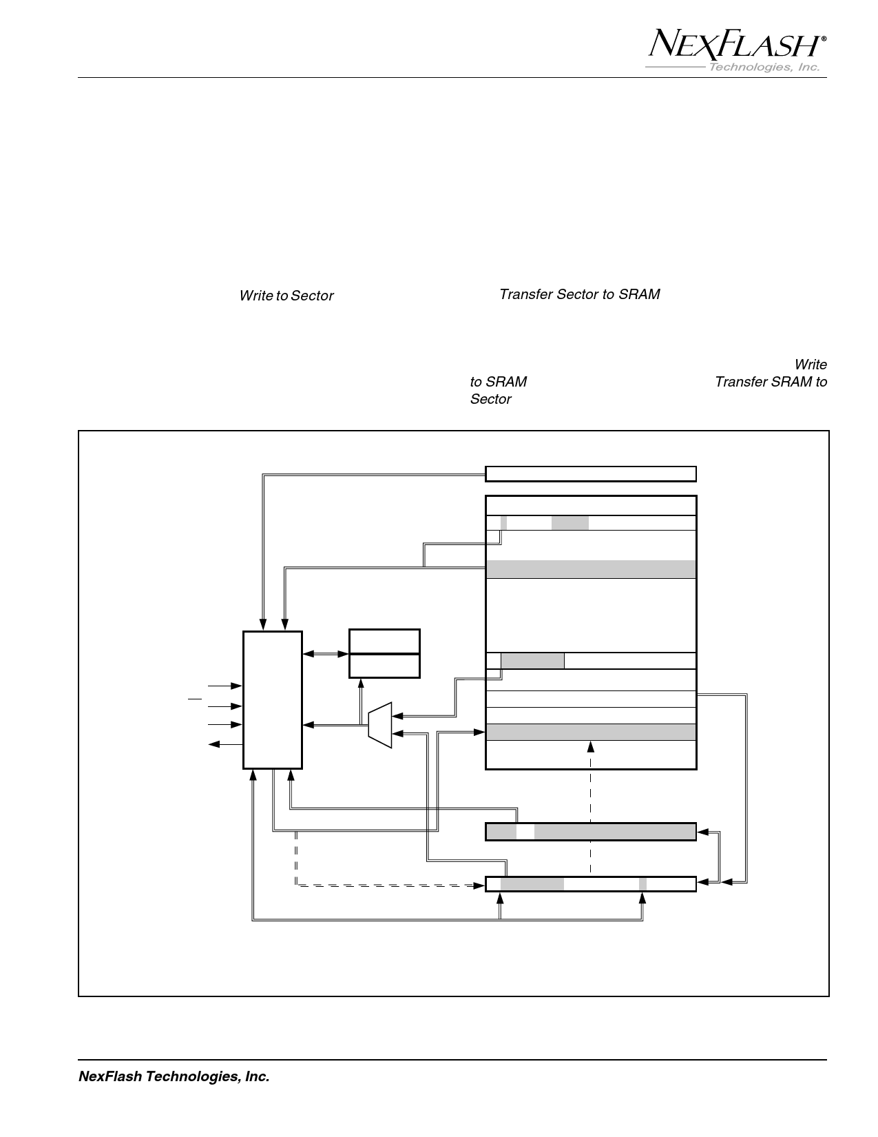
Serial SRAM and Program Buffer
One of the most powerful features of the NX25F011A and
NX25F041A is the integrated Serial SRAM and its associ-
ated Program Buffer. Together, the 264-byte Serial SRAM
and 264-byte Program Buffer provide up to 528-bytes of
usable SRAM storage. The SRAM can be used in
conjunction with the Flash memory or independently.
The main purpose of the Serial SRAM is to serve as the
primary buffer for data to be written into the Serial Flash
memory array. Using the Write to Sector command, data
is first shifted into the SRAM from the SPI bus. When the
command sequence has been completed, the entire
264-bytes is transferred to the Program Buffer. The
Program Buffer supports the array during the
Erase/Write cycle (tWP), freeing the SRAM to accept
new data. This double-buffering scheme increases
erase/write transfer rates and can eliminate the need for
external RAM buffers (Figure 5).
1
The SRAM is fully byte-addressable. Thus, the entire
264-bytes, a single byte, or a sequence of bytes can be
read from or written to the SRAM. This allows the SRAM to
2 be used as a temporary work area for read-modify-write
operations prior to a sector write.
The Transfer Sector to SRAM command allows the con-
3 tents of a specified sector of Flash memory to be moved to
the SRAM. This can be useful when only a portion of a sector
needs to be altered. In this case the sector is first transferred
to the SRAM, where modifications are made using the Write
4 to SRAM command. Once complete, a Transfer SRAM to
Sector command is used to update the sector.
READ FROM
DEVICE INFORMATION
SECTOR
READ FROM
SECTOR
DEVICE INFORMATION SECTOR
SCK
CS
SI
SO
SPI
COMMAND
AND
CONTROL
LOGIC
CONFIGURATION
REGISTER
STATUS
REGISTER
COMPARE SECTOR
TO SRAM
READ FROM
PROGRAM BUFFER
READ FROM
OR WRITE TO
SRAM
WRITE TO SECTOR
(VIA SRAM &
PROGRAM BUFFER)
SERIAL FLASH MEMORY ARRAY
512 AND 2048 BYTE-ADDRESSABLE
SECTORS OF 264-BYTES EACH
TRANSFER
SECTOR TO
SRAM
TRANSFER SRAM TO SECTOR
(VIA PROGRAM BUFFER)
TRANSFER SRAM TO
PROGRAM BUFFER
PROGRAM BUFFER
SERIAL SRAM
Note:
1. A single byte, several bytes, or all bytes of a Flash sector, the SRAM, or Program Buffer may be addressed.
2. All double lines represent implied connections or actions.
TRANSFER PROGRAM
BUFFER TO SRAM
5
6
7
8
9
10
11
12
Figure 5. Command Relationships of the SPI Interface, Serial Flash Memory Array, SRAM and Program Buffer
NexFlash Technologies, Inc.
5
PRELIMINARY NXSF014B-0699
06/11/99
Share Link: