TC4949 查看數據表(PDF) - TelCom Semiconductor Inc => Microchip
零件编号
产品描述 (功能)
生产厂家
TC4949 Datasheet PDF : 9 Pages
| |||
Multifunction Very Low Dropout Voltage Regulator
TC4949
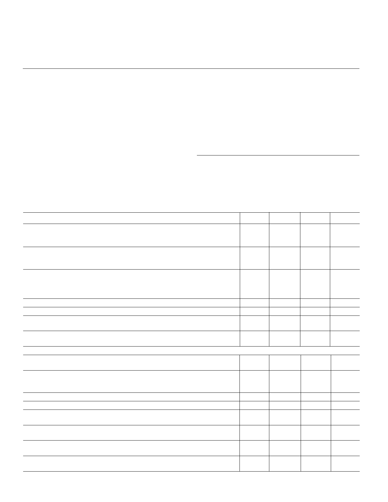
ABSOLUTE MAXIMUM RATINGS*
DC Operating Supply Voltage ......................... VCC = 28V
Transient Supply Voltage (T < 1.0 s) ........... VCC TR = 40V
Output Current ............................. IOUT (Internally Limited)
Output Voltage ............................................... VOUT = 20V
Sense Input Current ...................................... ISI = ±1.0mA
Sense Input Voltage ............................................ VSI =VCC
Output Voltages
Reset Output ........................................ VRESET = 20V
Sense Output ............................................. VSO = 20V
Output Currents
Reset Output ..................................... IRESET = 5.0mA
Sense Output ...........................................ISO = 5.0mA
Preregulator Output Voltage ............................. VZ = 7.0V
Preregulator Output Current ............................. IZ = 5.0mA
ESD Protection at any pin
Human Body Model .......................................... 2000V
Machine Model ................................................... 400V
Thermal Resistance, Junction–to–Air
P Suffix, DIP–8 Plastic Package,
Case 626 ............................................ ΘJA = 100°C/W
D Suffix, SO–8 Plastic Package,
Case 751 ............................................ ΘJA = 200°C/W
Maximim Junction Temperature ...................... TJ = 150°C
Storage Temperature Range .......... TSTG = -65 to +150°C
*This is a stress rating only, and functional operation of the device at these
or any other conditions beyond those indicated in the operation section of
the specifications is not implied. Exposure to absolute maximum ratings
conditions for extended periods of time may affect device reliability.
ELECTRICAL CHARACTERISTICS: (VCC = 14V, -40°C < TJ < 125°C, unless otherwise specified)
Symbol Parameter
Test Conditions
Min
Typ
Max
VOUT
VDROP
VIO
REGLINE
REGLOAD
ILIM
IQSE
IQ
RESET
VRESTH
VRESTH,HYS
TRESD
TRESR
VRESL
IRESH
VCTTH
VCTTH, HYS
Output Voltage
Dropout Voltage
Input to Output
Voltage Difference
in Undervoltage
Condition
Line Regulation
Load Regulation
Current Limit
Quiescent Current
TJ = 25°C, IOUT = 1.0mA
6.0V < VCC < 28V, 1.0mA < IOUT < 50mA
VCC = 35V, t < 1.0 s, 1.0mA < IOUT < 50mA
IOUT = 10mA
IOUT = 50mA
IOUT = 100mA
VCC = 4.0V, IOUT = 35mA
6.0V < VCC < 28V, IOUT = 1.0mA
1.0mA < IOUT < 100mA
VOUT = 4.5V
VOUT = 0V
IOUT = 0.3mA, TJ < 100°C
IOUT = 100mA
Reset Threshold
Voltage
Reset Threshold
Hysteresis
@TJ = 25°C
@TJ = -40 to +125°C
Reset Pulse Delay CT = 100nF, TR ≥ 100µs
Reset Reaction Time CT = 100nF
Reset Output
Low Voltage
Reset Output High
Leakage Current
RRESET = 10kΩ to VOUT , VCC ≥ 3.0V
VRESET = 5.0V
Delay Comparator
Threshold
Delay Comparator
Threshold Hysteresis
4.95
5.0
5.05
4.9
5.0
5.1
4.9
5.0
5.1
–
0.1
0.25
–
0.2
0.40
–
0.3
0.50
–
0.2
0.4
–
1.0
20
–
8.0
30
105
200
400
–
100
–
–
150
260
–
–
5.0
–
VOUT – 0.5
–
50
100
200
50
–
300
55
100
180
–
5.0
30
–
–
0.4
–
–
1.0
–
2.0
–
–
100
–
Units
V
V
V
mV
mV
mA
µA
mA
V
mV
ms
µs
V
µA
V
mV
TC4949-1 1/6/00
2
Share Link: 