TC4949 查看數據表(PDF) - TelCom Semiconductor Inc => Microchip
零件编号
产品描述 (功能)
生产厂家
TC4949 Datasheet PDF : 9 Pages
| |||
Multifunction Very Low Dropout Voltage Regulator
TC4949
OPERATING DESCRIPTION
The TC4949 is a monolithic integrated low dropout
voltage regulator. Several outstanding features and auxil-
iary functions are implemented to meet the requirements of
supplying microprocessor systems in automotive applica-
tions. Nevertheless, it is suitable also in other applications
where the present functions are required. The modular
approach of this device allows the use of other features and
functions independently when required.
VOUT
5.0V
VOUT
Voltage Regulator
The voltage regulator uses an isolated Collector Verti-
cal PNP transistor as a regulating element. With this struc-
ture, very low dropout voltage at currents up to 100mA is
obtained. The dropout operation of the standby regulator is
maintained down to 3.0V input supply voltage. The output
voltage is regulated up to the transient input supply voltage
of 35V. With this feature no functional interruption due to
overvoltage pulses is generated.
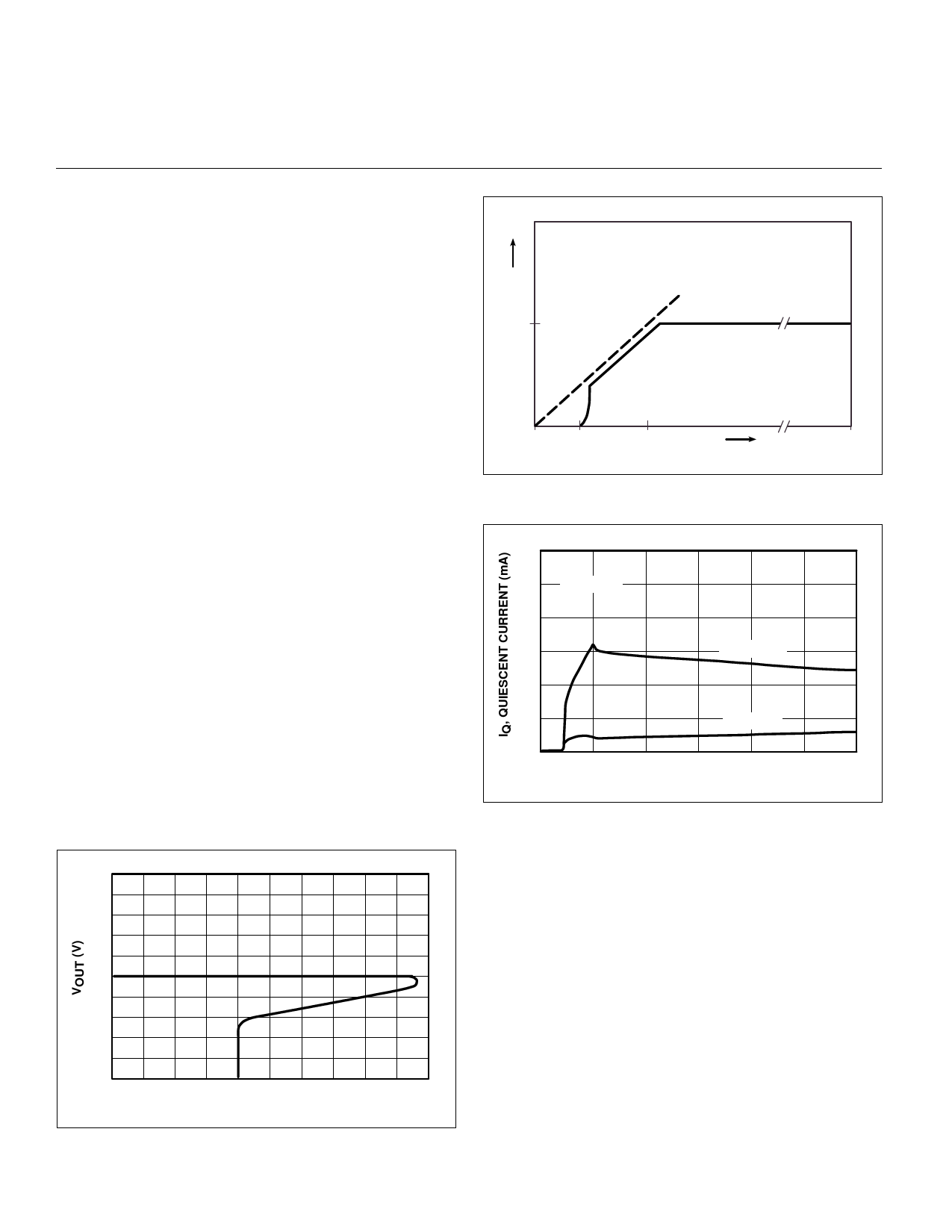
The typical curve showing the standby output voltage as
a function of the input supply voltage is shown in Figure 13.
The current consumption of the device (quiescent cur-
rent) is less than 200µA.
To reduce the quiescent current peak in the undervoltage
region and to improve the transient response in this region,
the dropout voltage is controlled. The quiescent current as
a function of the supply input voltage is shown in Figure 14.
Short Circuit Protection:
The maximum output current is internally limited. In
case of short circuit, the output current is foldback current
limited as described in Figure 12.
0V 2.0V
5.0V
35V
VCC
Figure 13. Output Voltage versus Supply Voltage
3.0
2.5 TJ = 25˚C
2.0
1.5
RL = 100Ω
1.0
0.5
RL = 5.0k
0
0
5.0
10
15
20
25
30
VCC, SUPPLY VOLTAGE (V)
Figure 14. Quiescent Current versus Supply Voltage
10
5.0
0
20
100
200
IOUT (mA)
Figure 12. Foldback Characteristic of VOUT
Preregulator
To improve the transient immunity a preregulator stabi-
lizes the internal supply voltage to 6.0V. This internal voltage
is present at Pin 3 (VZ ). This voltage should not be used as
an output because the output capability is very small
(≤ 100µA).
This output may be used as an option when better
transient behavior for supply voltages less than 8.0V is
required. In this case a capacitor (100nF – 1.0µF) must be
connected between Pin 3 and Gnd. If this feature is not used
Pin 3 must be left open.
TC4949-1 1/6/00
6
Share Link: 