STLC7550TQFP 查看數據表(PDF) - STMicroelectronics
零件编号
产品描述 (功能)
生产厂家
STLC7550TQFP Datasheet PDF : 17 Pages
| |||
STLC7550
PIN DESCRIPTION (continued)
4 - ANALOG INTERFACE (9 pins)
4.1 - DAC and ADC Positive Reference
Voltage Output (VREFP)
This pin provides the Positive Reference Voltage
used by the 16-bit converters. The reference volt-
age, VREF, is the voltage difference between the
VREFP and VREFN outputs, and its nominal value is
1.25V. VREFP should be externally decoupled with
respect to VCM.
4.2 - DAC and ADC Negative Reference
Voltage Output (VREFN)
This pin provides the Negative Reference Voltage
used by the 16-bit converters, and should be exter-
nally decoupled with respect to VCM.
4.3 - Common Mode Voltage Output (VCM)
This output pin is the common mode voltage
(AVDD - AGND)/2. This output must be decoupled
with respect to GND.
4.4 - Non-inverting Smoothing Filter Output(OUT+)
This pin is the non-inverting output of the fully
differential analog smoothing filter.
4.5 - Inverting Smoothing Filter Output (OUT-)
This pin is the inverting output of the fully differential
analog smoothing filter. Outputs OUT+ and OUT-
provide analog signals with maximum peak-to-
peak amplitude 2 x VREF, and must be followed by
an external two pole smoothing filter. The external
filter follows the internal single pole switch capaci-
tor filter. The cutoff frequency of the external filter
must be greater than two times the sampling fre-
quency (FS), so that the combined frequency re-
sponse of both the internal and external filters is flat
in the passband . The attenuator of the last output
stage can be programmed to 0dB, 6dB or infinite.
4.6 - Non-inverting Analog Input (IN+)
This pin is the differential non-inverting ADC input.
4.7 - Inverting Analog Input (IN-)
This pin is the differential inverting ADC input.
These analog inputs (IN+, IN-) are presented to the
Sigma-Delta modulator. The analog input peak-to-
peak differential signal range must be less than
2 x VREF, and must be preceded by an external
single pole anti-aliasing filter. The cut-off frequency
of the filter must be lower than one half the over-
sampling frequency. These filters should be set as
close as possible to the IN+ and IN- pins. The gain
of the first stage is programmable (see Table 3).
4.8 - Non-inverting Auxiliary Analog
Input (AUX IN+)
This pin is the differential non-inverting auxiliary ADC
input. The characteristics are same as the IN+ input.
4.9 - Inverting Auxiliary Analog Input (AUX IN-)
This pin is the differential inverting auxiliary ADC
input. The characteristics are same as the IN- input.
The input pair (IN+/IN- or AUX IN+/AUX IN-) are
software selectable.
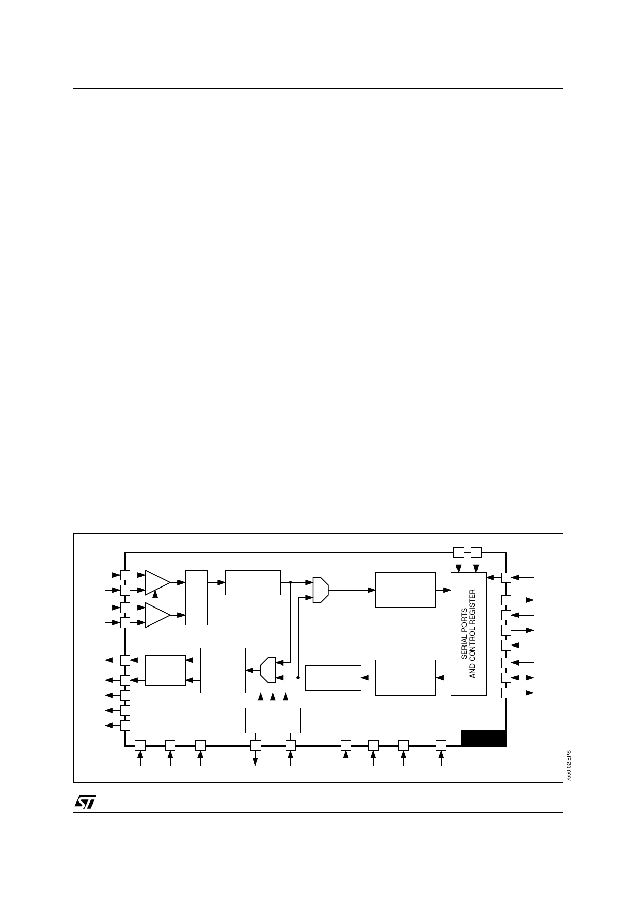
BLOCK DIAGRAM (TQFP44)
HC0 HC1
15 14
IN+
IN-
AUXIN+
AUXIN-
OUT+
OUT-
VREFP
VREFN
VCM
27
ANALOG
28
MODULATOR
MUX
25
26
(0 + 6dB in
diff. input)
36
ATTEN.
0dB/+6dB/
37
INFINITE
18
DAC 1 BIT
First order
differential
switched
capacitor
filter
19
CLOCK
30
GENERATOR
2nd ORDER
MODULATOR
LOW-PASS
(0.425 x sampling
frequency)
LOW-PASS
(0.425 x sampling
frequency)
29
20
31
8
9
5
6
38
16
7
42
41
40
39
17
4
3
STLC7550
MCM
DOUT
DIN
TSTD1
TS
M/S
FS
SCLK
AVDD AGND1 AGND2
XTALOUT XTALIN
DVDD DGND RESET PWRDWN
5/17
Share Link: 