ICX058AL 查看數據表(PDF) - Sony Semiconductor
零件编号
产品描述 (功能)
生产厂家
ICX058AL Datasheet PDF : 17 Pages
| |||
ICX058AL
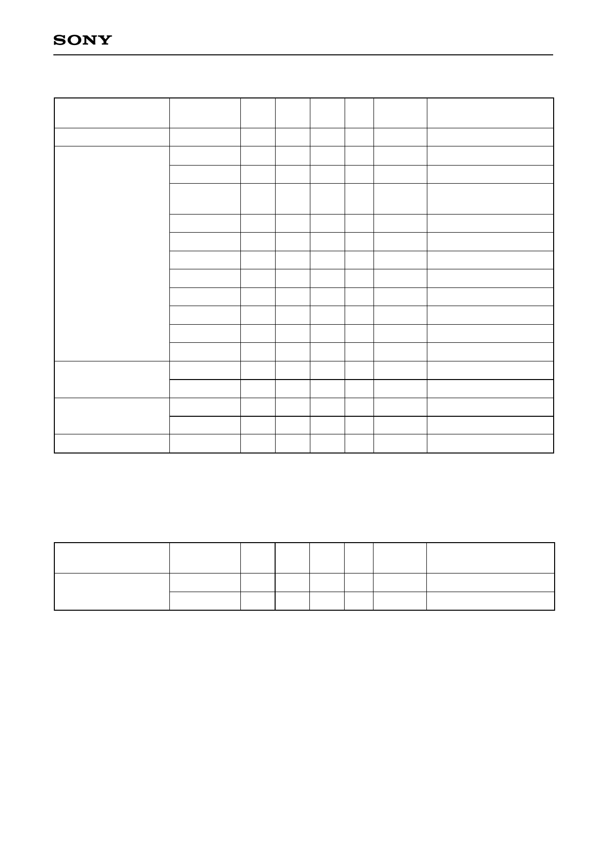
Clock Voltage Conditions
Item
Symbol
Min.
Typ.
Max.
Unit
Waveform
diagram
Remarks
Readout clock voltage VVT
14.55 15.0 15.45 V
1
VVH1, VVH2 –0.05 0 0.05 V
2
VVH = (VVH1 + VVH2)/2
VVH3, VVH4
–0.2 0 0.05 V
2
VVL1, VVL2,
VVL3, VVL4
–9.0 –8.5 –8.0 V
2
VVL = (VVL3 + VVL4)/2
VφV
7.8 8.5 9.05 V
2
VφV = VVHn–VVLn (n = 1 to 4)
Vertical transfer clock
voltage
I VVH1 – VVH2 I
VVH3 – VVH –0.25
VVH4 – VVH –0.25
0.1 V
2
0.1 V
2
0.1 V
2
VVHH
0.5 V
2
High-level coupling
VVHL
0.5 V
2
High-level coupling
VVLH
0.5 V
2
Low-level coupling
Horizontal transfer
clock voltage
Reset gate clock
voltage
VVLL
0.5 V
VφH, VφLH
4.75 5.0 5.25 V
VHL, VLHL
–0.05 0 0.05 V
VφRG
4.5 5.0 5.5 V
VRGLH – VRGLL
0.8 V
2
Low-level coupling
3
∗5
3
∗5
4
∗6
4
Low-level coupling
Substrate clock voltage VφSUB
22.5 23.5 24.5 V
5
∗5 The horizontal final stage transfer clock input pin LHφ1 is connected to the horizontal transfer clock input
pin Hφ1.
∗6 The reset gate clock voltage need not be adjusted when reset gate clock is driven when the specifications
are as given below. In this case, the reset gate clock voltage setting indicated on the back of the image
sensor has not significance.
Item
Reset gate clock
voltage
Symbol
VRGL
VφRG
Min.
Typ.
Max.
Unit
Waveform
diagram
–0.2 0 0.2 V
4
8.5 9.0 9.5 V
4
Remarks
–4–
Share Link: 