MC34072AP 查看數據表(PDF) - Motorola => Freescale
零件编号
产品描述 (功能)
生产厂家
MC34072AP Datasheet PDF : 20 Pages
| |||
MC34071,2,4,A MC33071,2,4,A
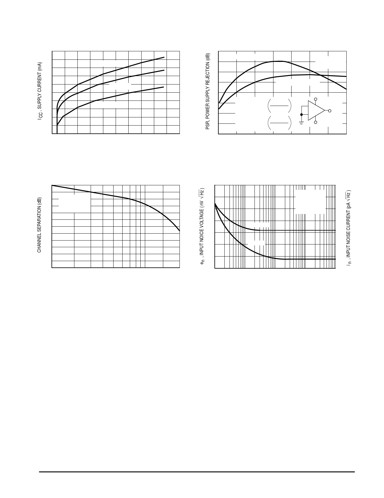
Figure 33. Supply Current versus
Supply Voltage
9.0
8.0
TA = –55°C
7.0
TA = 25°C
6.0
TA = 125°C
5.0
4.0
0
5.0
10
15
20
25
VCC, |VEE|, SUPPLY VOLTAGE (V)
Figure 34. Power Supply Rejection
versus Temperature
105
–PSR (∆VEE = +1.5 V)
95
VCC = +15 V
VEE = –15 V
85
75
65
–55
+PSR (∆VCC = +1.5 V)
+PSR = 20 Log
–PSR = 20 Log
∆VO/ADM
∆VCC
∆VO/ADM
∆VEE
∆VCC
–
ADM
+
∆VO
∆VEE
–25
0
25 50
75 100 125
TA, AMBIENT TEMPERATURE (°C)
Figure 35. Channel Separation versus Frequency
120
100 VCC = +15 V
VEE = –15 V
80 TA = 25°C
60
40
20
0
10
20 30
50 70 100 200 300
f, FREQUENCY (kHz)
Figure 36. Input Noise versus Frequency
70
2.8
60
VCC = +15 V
VEE = –15 V
2.4
50
VCM = 0
TA = 25°C
2.0
40
1.6
Voltage
30
1.2
20
Current
0.8
10
0.4
0
0
10
100
1.0 k
10 k
100 k
f, FREQUENCY (kHz)
APPLICATIONS INFORMATION
CIRCUIT DESCRIPTION/PERFORMANCE FEATURES
Although the bandwidth, slew rate, and settling time of the
MC34071 amplifier series are similar to op amp products
utilizing JFET input devices, these amplifiers offer other
additional distinct advantages as a result of the PNP
transistor differential input stage and an all NPN transistor
output stage.
Since the input common mode voltage range of this input
stage includes the VEE potential, single supply operation is
feasible to as low as 3.0 V with the common mode input
voltage at ground potential.
The input stage also allows differential input voltages up to
±44 V, provided the maximum input voltage range is not
exceeded. Specifically, the input voltages must range
between VEE and VCC supply voltages as shown by the
maximum rating table. In practice, although not
recommended, the input voltages can exceed the VCC
voltage by approximately 3.0 V and decrease below the VEE
voltage by 0.3 V without causing product damage, although
output phase reversal may occur. It is also possible to source
up to approximately 5.0 mA of current from VEE through
either inputs clamping diode without damage or latching,
although phase reversal may again occur.
If one or both inputs exceed the upper common mode
voltage limit, the amplifier output is readily predictable and
may be in a low or high state depending on the existing input
bias conditions.
10
MOTOROLA ANALOG IC DEVICE DATA
Share Link: 