M41T11 查看數據表(PDF) - STMicroelectronics
零件编号
产品描述 (功能)
生产厂家
M41T11 Datasheet PDF : 30 Pages
| |||
M41T11
Operation
2.3
Write mode
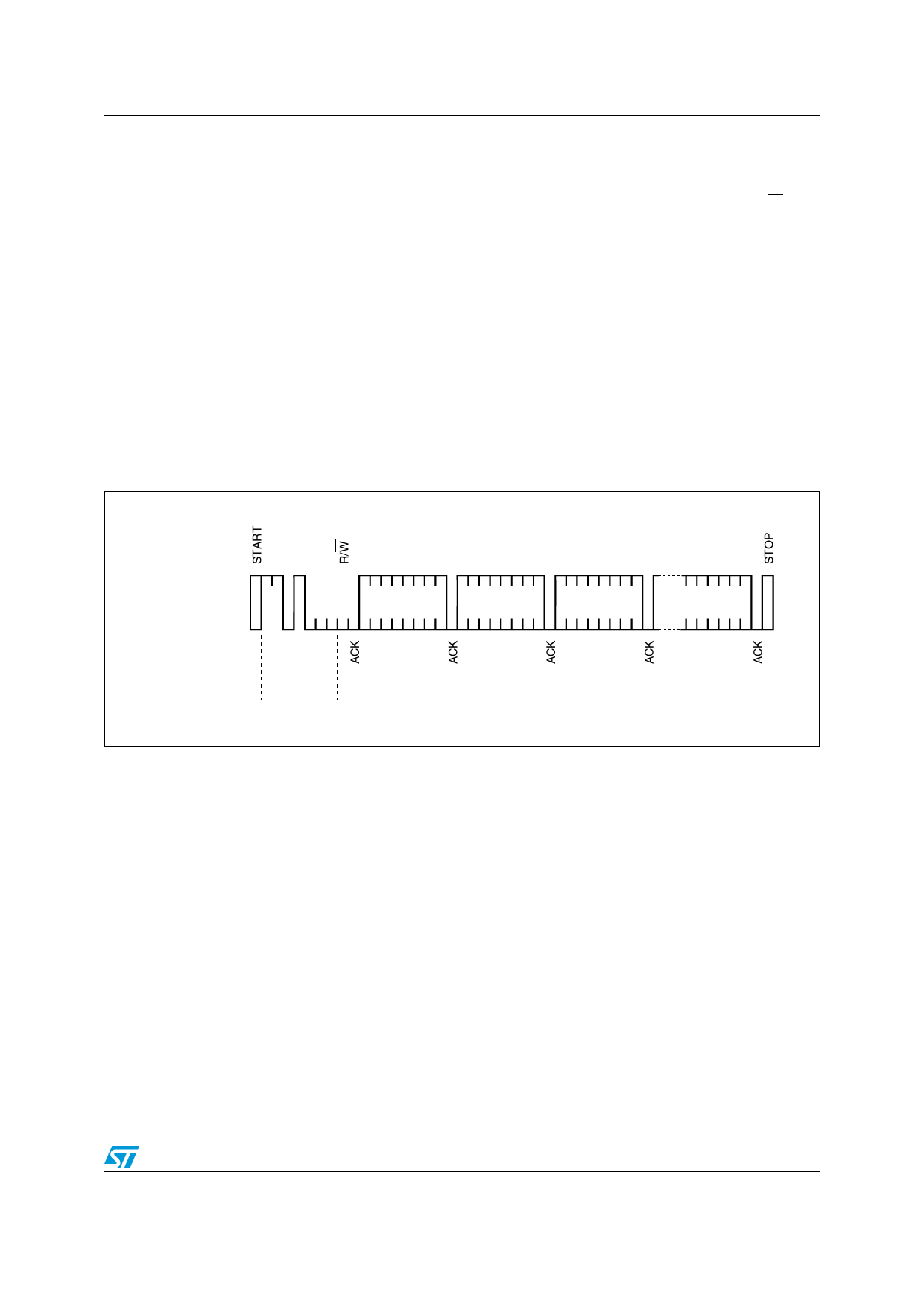
In this mode the master transmitter transmits to the M41T11 slave receiver. Bus protocol is
shown in Figure 11. Following the START condition and slave address, a logic '0' (R/W = 0)
is placed on the bus and indicates to the addressed device that word address An will follow
and is to be written to the on-chip address pointer. The data word to be written to the
memory is strobed in next and the internal address pointer is incremented to the next
memory location within the RAM on the reception of an acknowledge clock. The M41T11
slave receiver will send an acknowledge clock to the master transmitter after it has received
the slave address and again after it has received the word address and each data byte.
2.4
Data retention mode
With valid VCC applied, the M41T11 can be accessed as described above with read or write
cycles. Should the supply voltage decay, the M41T11 will automatically deselect, write
protecting itself when VCC falls (see Figure 15).
Figure 11. Write mode sequence
BUS ACTIVITY:
MASTER
SDA LINE
S
WORD
ADDRESS (An)
BUS ACTIVITY:
SLAVE
ADDRESS
DATA n
DATA n+1
DATA n+X P
AI00591
Doc ID 6103 Rev 10
13/30
Share Link: 