MC74HC173N 查看數據表(PDF) - Motorola => Freescale
零件编号
产品描述 (功能)
生产厂家
MC74HC173N Datasheet PDF : 6 Pages
| |||
MC74HC173
PIN DESCRIPTIONS
INPUTS
D0, D1, D2, D3 (Pins 14, 13, 12, 11)
4–bit data inputs. Data on these pins, when enabled by the
Data–Enable Controls, are entered into the flip–flops on the
rising edge of the clock.
CLOCK (Pin 7)
Clock input.
OUTPUTS
Q0, Q1, Q2, Q3 (Pins 3, 4, 5, 6)
3–state register outputs. During normal operation of the
device, the outputs of the D flip–flops appear at these pins.
During 3–state operation, these outputs assume a high–
impedance state.
CONTROL INPUT
Reset (Pin 15)
Asynchronous reset input. A high level on this pin resets all
flip–flops and forces the Q outputs low, if they are not already
in high–impedance state.
DE1, DE2 (Pins 9, 10)
Active–low Data Enable Control inputs. When both Data
Enable Controls are low, data at the D inputs are loaded into
the flip–flops with the rising edge of the Clock input. When
either or both of these controls are high, there is no change in
the state of the flip–flops, regardless of any changes at the D
or Clock inputs.
OE1, OE2 (Pins 1, 2)
Output Enable Control inputs. When either or both of the
Output Enable Controls are high, the Q outputs of the device
are in the high–impedance state. When both controls are
low, the device outputs display the data in the flip–flops.
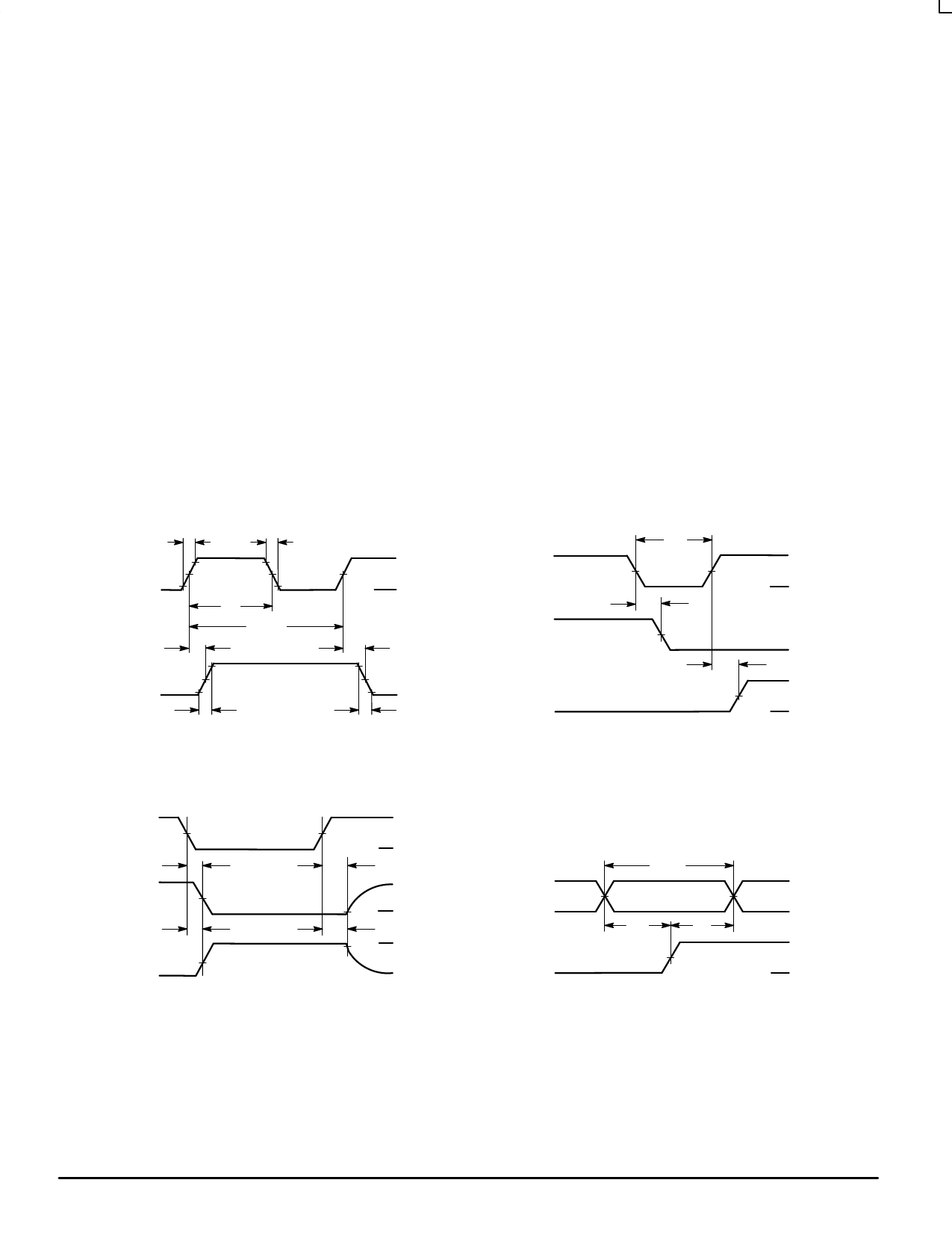
SWITCHING WAVEFORMS
tr
tf
CLOCK
90%
50%
VCC
10%
GND
tw
1/fmax
tPLH
tPHL
90%
Q 50%
10%
tTLH
tTHL
tw
VCC
RESET
50%
GND
tPHL
Q
CLOCK
50%
trec
VCC
50%
GND
Figure 1.
Figure 2.
VCC
OE
50%
GND
tPZL tPLZ
Q
50%
HIGH
IMPEDANCE
10% VOL
INPUT D
OR DE
VALID
50%
VCC
GND
tPZH tPHZ
tsu
th
90% VOH
VCC
Q
50%
HIGH
CLOCK
50%
GND
IMPEDANCE
Figure 3.
Figure 4.
MOTOROLA
4
High–Speed CMOS Logic Data
DL129 — Rev 6
Share Link: 