AD621(RevA) 查看數據表(PDF) - Analog Devices
零件编号
产品描述 (功能)
生产厂家
AD621 Datasheet PDF : 16 Pages
| |||
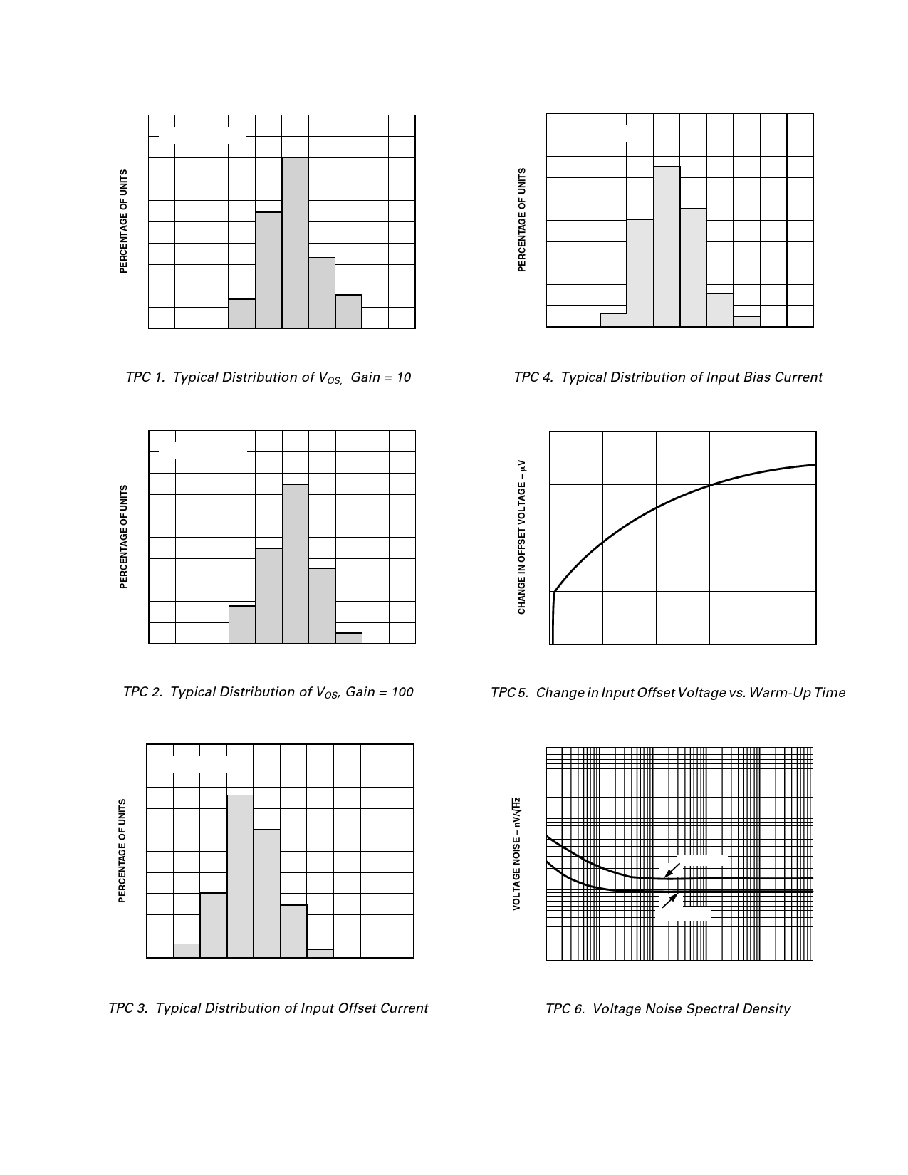
50
SAMPLE SIZE = 90
40
30
20
10
0
–200
–100
0
+100
INPUT OFFSET VOLTAGE – µV
+200
Figure 1. Typical Distribution of VOS, Gain = 10
50
SAMPLE SIZE = 90
40
30
20
10
0
–80
–40
0
+40
+80
INPUT OFFSET VOLTAGE – µV
Figure 2. Typical Distribution of VOS, Gain = 100
50
SAMPLE SIZE = 90
40
30
20
10
0
–400
–200
0
+200
INPUT OFFSET CURRENT – pA
+400
Figure 3. Typical Distribution of Input Offset Current
Typical Characteristics–AD621
50
SAMPLE SIZE = 90
40
30
20
10
0
–800
–400
0
+400
INPUT BIAS CURRENT – pA
+800
Figure 4. Typical Distribution of Input Bias Current
2
1.5
1
0.5
0
0
1
2
3
4
5
WARM-UP TIME – Minutes
Figure 5. Change in Input Offset Voltage vs. Warm-Up Time
1000
100
GAIN = 10
10
GAIN = 100
1
1
10
100
1k
10k
100k
FREQUENCY – Hz
Figure 6. Voltage Noise Spectral Density
REV. A
–5–
Share Link: 