ATF-34143 查看數據表(PDF) - Agilent Technologies, Inc
零件编号
产品描述 (功能)
生产厂家
ATF-34143 Datasheet PDF : 15 Pages
| |||
ATF-34143 Typical Scattering Parameters, VDS = 3 V, IDS = 20 mA
Freq.
S11
S21
S12
GHz Mag. Ang. dB Mag. Ang. dB Mag. Ang.
0.5 0.96 -37 20.07 10.079 153 -29.12 0.035 68
0.8 0.91 -60 19.68 9.642 137 -26.02 0.050 56
1.0 0.87 -76 18.96 8.867 126 -24.29 0.061 48
1.5 0.81 -104 17.43 7.443 106 -22.27 0.077 34
1.8 0.78 -115 16.70 6.843 98 -21.62 0.083 28
2.0 0.75 -126 16.00 6.306 90 -21.11 0.088 23
2.5 0.72 -145 14.71 5.438 75 -20.45 0.095 15
3.0 0.69 -162 13.56 4.762 62 -19.83 0.102
7
4.0 0.65 166 11.61 3.806 38 -19.09 0.111 -8
5.0 0.64 139 10.01 3.165 16 -18.49 0.119 -21
6.0 0.65 114 8.65 2.706 -5 -18.06 0.125 -35
7.0 0.66
89 7.33 2.326 -27 -17.79 0.129 -49
8.0 0.69
67 6.09 2.017 -47 -17.52 0.133 -62
9.0 0.72
48 4.90 1.758 -66 -17.39 0.135 -75
10.0 0.75
30 3.91 1.568 -86 -17.08 0.140 -88
11.0 0.77
10 2.88 1.393 -105 -16.95 0.142 -103
12.0 0.80 -10 1.74 1.222 -126 -16.95 0.142 -118
13.0 0.83 -29 0.38 1.045 -145 -17.39 0.135 -133
14.0 0.85 -44 -0.96 0.895 -161 -17.86 0.128 -145
15.0 0.86 -55 -2.06 0.789 -177 -18.13 0.124 -156
16.0 0.85 -72 -3.09 0.701 166 -18.13 0.124 -168
17.0 0.85 -88 -4.22 0.615 149 -18.06 0.125 177
18.0 0.88 -101 -5.71 0.518 133 -18.94 0.113 165
S22
Mag. Ang.
0.40 -35
0.34 -56
0.32 -71
0.29 -98
0.28 -110
0.26 -120
0.25 -140
0.23 -156
0.22 174
0.22 146
0.23 118
0.25
91
0.29
67
0.34
46
0.39
28
0.43
10
0.47 -10
0.53 -28
0.58 -42
0.62 -57
0.65 -70
0.68 -85
0.71 -103
MSG/MAG
dB
24.59
22.85
21.62
19.85
19.16
18.55
17.58
16.69
15.35
14.25
13.35
10.91
9.71
8.79
8.31
7.56
6.83
6.18
5.62
5.04
3.86
3.00
2.52
ATF-34143 Typical Noise Parameters
VDS = 3 V, IDS = 20 mA
Freq.
Fmin
Γopt
Rn/50
Ga
GHz
dB
Mag.
Ang.
-
dB
0.5
0.10
0.90
13
0.16
21.8
0.9
0.11
0.85
27
0.14
18.3
1.0
0.11
0.84
31
0.13
17.8
1.5
0.14
0.77
48
0.11
16.4
1.8
0.17
0.74
57
0.10
16.0
2.0
0.19
0.71
66
0.09
15.6
2.5
0.23
0.65
83
0.07
14.8
3.0
0.29
0.59
102
0.06
14.0
4.0
0.42
0.51
138
0.03
12.6
5.0
0.54
0.45
174
0.03
11.4
6.0
0.67
0.42
-151
0.05
10.3
7.0
0.79
0.42
-118
0.10
9.4
8.0
0.92
0.45
-88
0.18
8.6
9.0
1.04
0.51
-63
0.30
8.0
10.0
1.16
0.61
-43
0.46
7.5
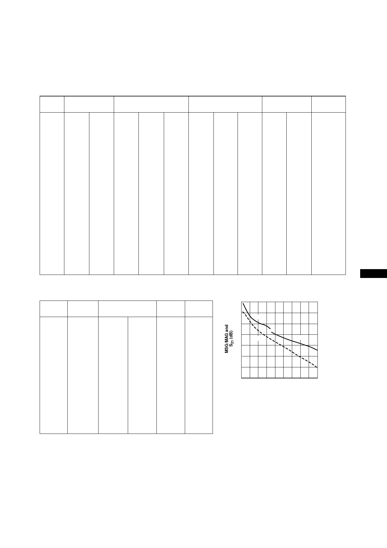
25
20
MSG
15
10
S21
5
MAG
0
-5
-10
0 2 4 6 8 10 12 14 16 18
FREQUENCY (GHz)
Figure 23. MSG/MAG and |S21|2 vs.
Frequency at 3 V, 20 mA.
Notes:
1. Fmin values at 2 GHz and higher are based on measurements while the Fmins below 2 GHz have been extrapolated. The Fmin values
are based on a set of 16 noise figure measurements made at 16 different impedances using an ATN NP5 test system. From these
measurements a true Fmin is calculated. Refer to the noise parameter application section for more information.
2. S and noise parameters are measured on a microstrip line made on 0.025 inch thick alumina carrier. The input reference plane is at the
end of the gate lead. The output reference plane is at the end of the drain lead. The parameters include the effect of four plated
through via holes connecting source landing pads on top of the test carrier to the microstrip ground plane on the bottom side of the
carrier. Two 0.020 inch diameter via holes are placed within 0.010 inch from each source lead contact point, one via on each side of
that point.
7
Share Link: 