SK10LVE111PJT 查看數據表(PDF) - Semtech Corporation
零件编号
产品描述 (功能)
生产厂家
SK10LVE111PJT Datasheet PDF : 6 Pages
| |||
SK10/100LVE111
1:9 Differential LVECL/LVPECL
Clock Driver
HIGH-PERFORMANCE PRODUCTS
Description
The SK10/100LVE111 is a low skew 1-to-9 differential
driver designed with clock distribution in mind. The
SK10/100LVE111’s function and performance are
similar to the SK100E111, with the added feature of
low voltage operation and the enable input. It accepts
one signal input which can be either differential or
single-ended if the VBB output is used. The signal is
fanned out to 9 identical differential outputs.
The device is specifically designed, modeled, and
produced with low skew as the key goal. Optimal
design and layout serve to minimize gate-to-gate skew
within a device, and characterization is used to
determine process control limits that ensure consistent
tpd distributions from lot to lot. The net result is a
dependable, guaranteed low skew device.
To ensure that the tight skew specification is met, it
is necessary that both sides of the differential output
are terminated into 50W, even if only one side is being
used. In most applications, all nine differential pairs
will be used and therefore terminated. In the case
where fewer than nine pairs are used, it is necessary
to terminate at least the output pairs on the same
package side as the pair(s) being used on that side in
order to maintain minimum skew. Failure to do so will
result in small degradations of propagation delay (on
the order of 10–20ps) of the output(s) being used
which, while not being catastrophic to most designs,
will mean a loss of skew margin.
The SK10/100LVE111, as with most other ECL devices,
can be operated from a positive VCC supply in PECL
mode. This allows the LVE111 to be used for high
performance clock distribution in +3.3V systems.
Designers can take advantage of the LVE111’s
performance to distribute low skew clocks across the
back plane or the board. In a PECL environment, series
or Thevenin line terminations are typically used as
they require no additional power supplies. For systems
incorporating GTL, parallel termination offers the lowest
power by taking advantage of the 1.2V supply as a
terminating voltage.
The SK10/100LVE111 provides VBB output for either
single-ended use or as a DC bias for AC coupling to
the device. The VBB output pin should be used only
as a DC bias for the LVE111 as its current sink/source
capability is limited. Whenever used, the VBB pin
should be bypassed to VCC via a 0.01 µF capacitor.
Features
• 200 ps Part-to-Part Skew
• 50 ps Output-to-Output Skew
• Differential Design
• VBB Output
• Voltage and Temperature Compensated Outputs
• Low Voltage VEE Range of –3.0 to –3.8V
• 75KW Internal Input Pulldown Resistors
• Fully Compatible with MC100LVE111
• Specified Over Industrial Temperature Range:
–40oC to 85oC
• ESD Protection of >4000V
• Available in 28-pin PLCC Package
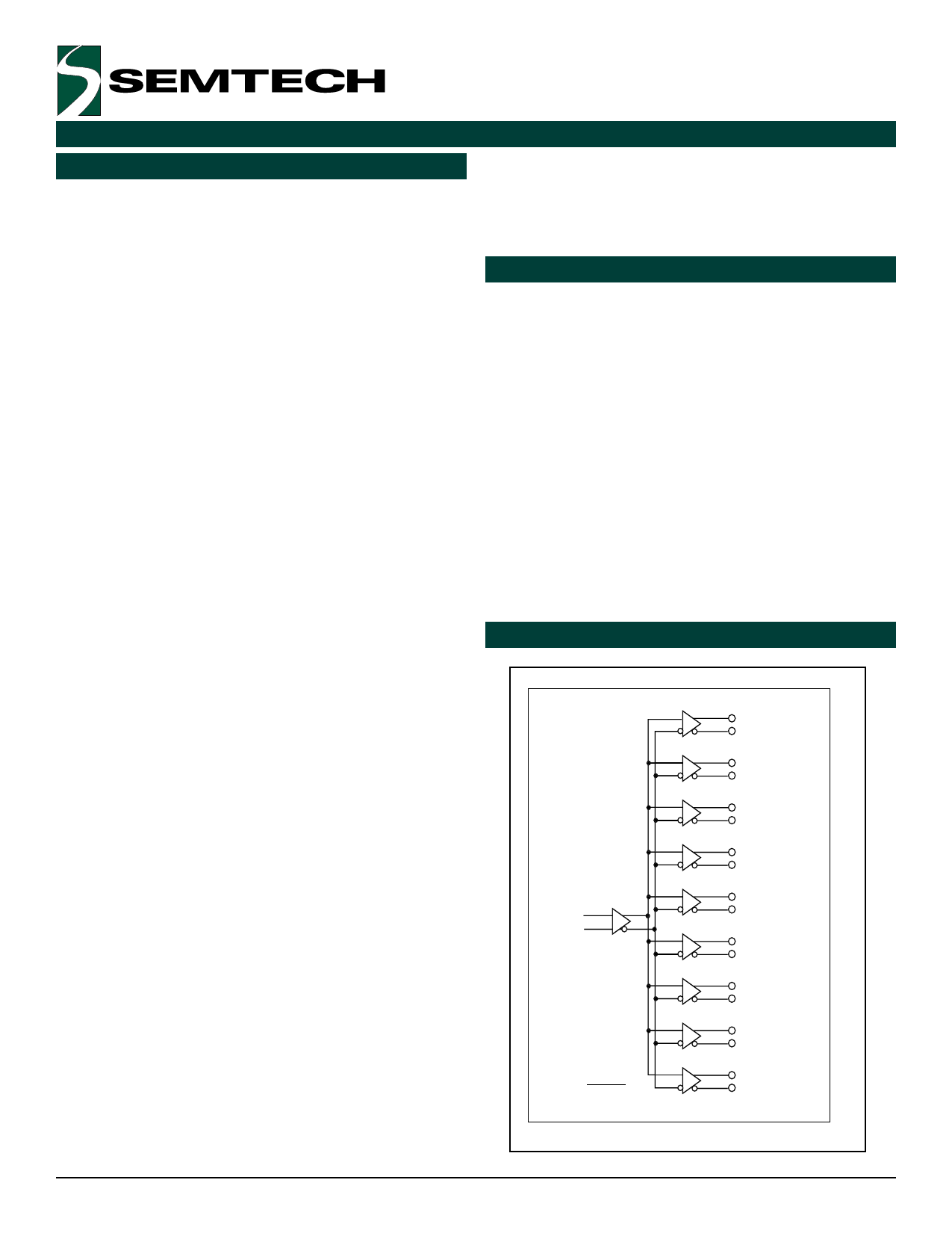
Functional Block Diagram
Q0
Q0*
Q1
Q1*
Q2
Q2*
Q3
Q3*
Q4
Q4*
IN
IN*
Q5
Q5*
Q6
Q6*
Q7
Q7*
VBB
Q8
Q8*
Revision 1/August 27, 2001
1
www.semtech.com
Share Link: 