ICS673M-01LFT 查看數據表(PDF) - Integrated Device Technology
零件编号
产品描述 (功能)
生产厂家
ICS673M-01LFT Datasheet PDF : 9 Pages
| |||
ICS673-01
PLL BUILDING BLOCK
PLL BUILDING BLOCK
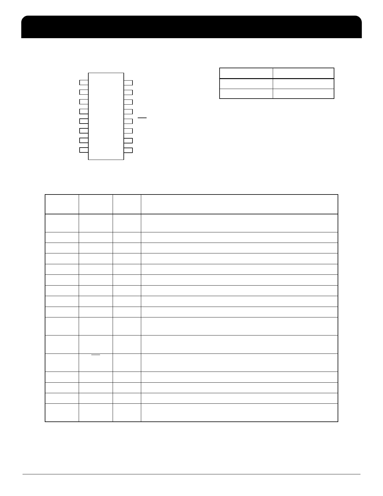
Pin Assignment
F B IN
1
VDD
2
VDD
3
GND
4
GND
5
GND
6
CHGP
7
VC O IN
8
16
R EFIN
15
NC
14
CLK1
13
CLK2
12
PD
11
SEL
10
OE
9
CAP
VCO Predivide Select Table
SEL
VCO Predivide
0
4
1
1
0 = connect pin directly to ground
1 = connect pin directly to VDD
16 pin narrow (150 m il) S O IC
Pin Descriptions
Pin
Number
1
2
3
4
5
6
7
8
9
10
11
12
13
14
15
16
Pin
Name
FBIN
VDD
VDD
GND
GND
GND
CHGP
VCOIN
CAP
OE
SEL
PD
CLK2
CLK1
NC
REFIN
Pin
Type
Pin Description
Input Feedback clock input. Connect the feedback clock to this pin.
Triggered on falling edge.
Power Connect to +3.3 V or +5 V and to VDD on pin 3.
Power Connect to VDD on pin 2.
Power Connect to ground.
Power Connect to ground.
Power Connect to ground.
Output Charge pump output. Connect to VCOIN under normal operation.
Input Input to internal VCO.
Input Loop filter return.
Input Output enable. Active when high. Tri-states both outputs when low.
Internal weak pull-up resistor.
Input Select pin for VCO predivide to feedback divider per table above.
Internal weak pull-up resistor.
Input Power down. Turns off entire chip when pin is low. Outputs stop low.
Internal weak pull-up resistor.
Output Clock output 2. Low skew divide by two version of CLK1.
Output Clock output 1.
- No connect. Nothing is connected internally to this pin.
Input Reference input. Connect reference clock to this pin. Triggered on
falling edge.
IDT™ / ICS™ PLL BUILDING BLOCK
2
ICS673-01 REV Q 071906
Share Link: 