BR24C01A-W 查看數據表(PDF) - ROHM Semiconductor
零件编号
产品描述 (功能)
生产厂家
BR24C01A-W Datasheet PDF : 13 Pages
| |||
Memory ICs
BR24C01A-W / BR24C01AF-W / BR24C01AFJ-W / BR24C01AFV-W / BR24C02-W / BR24C02F-W /
BR24C02FJ-W / BR24C02FV-W / BR24C04-W / BR24C04F-W / BR24C04FJ-W / BR24C04FV-W
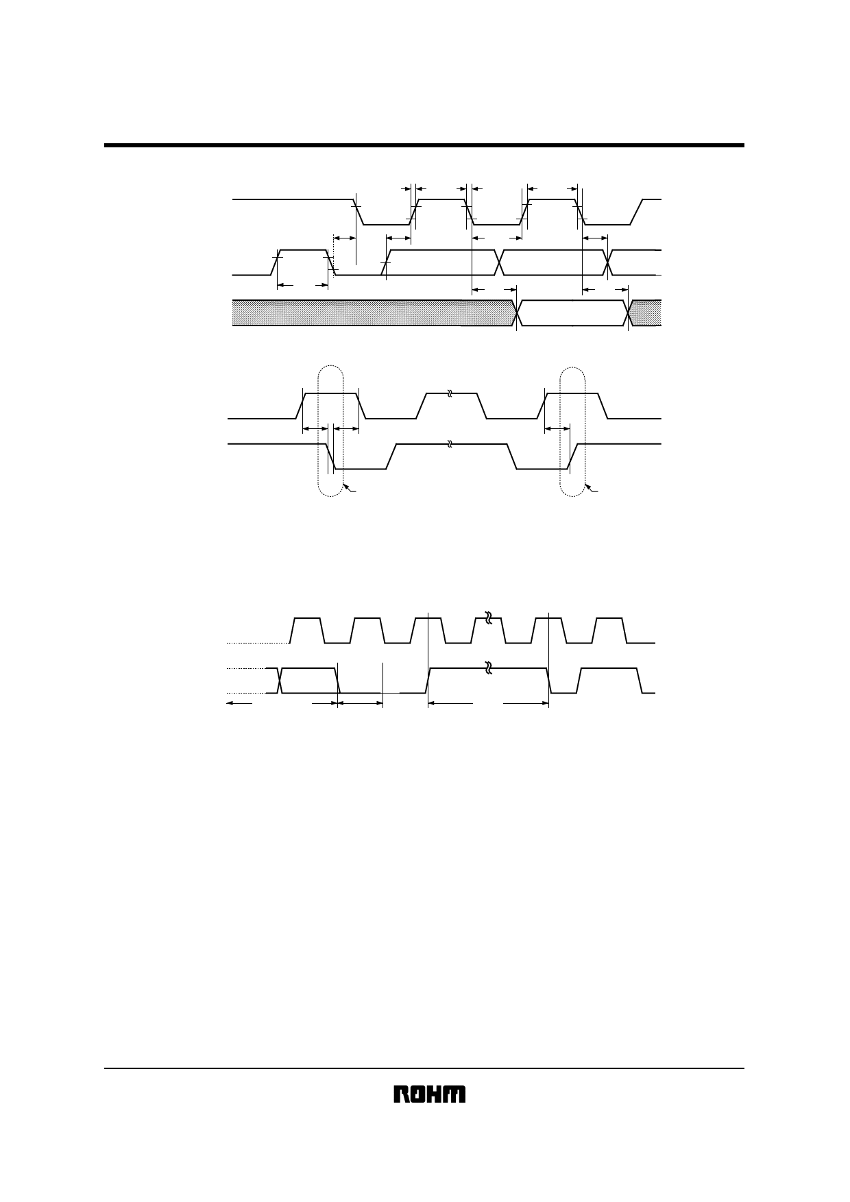
!Timing charts
SCL
SDA
(input)
SDA
(output)
tHD : STA
tBUF
tR
tF
tHIGH
tSU : DAT
tLOW
tHD : DAT
tPD
tDH
SCL
SDA
tSU : STA
tHD : STA
tSU : STO
START BIT
STOP BIT
· Data is read on the rising edge of SCL.
· Data is output in synchronization with the falling edge of SCL.
Fig.1 Synchronized data input / output timing
SCL
SDA
D0
Write data
(n address)
ACK
tWR
Stop condition
Start condition
Fig.2 Write cycle timing
!Circuit operation
(1) Start condition (recognition of start bit)
Before executing any command, when SCL is HIGH, a start condition (start bit) is required to cause SDA to fall from
HIGH to LOW. This IC is designed to constantly detect whether there is a start condition (start bit) for the SDA and
SCL line, and no commands will be executed unless this condition is satisfied.
(See Fig.1 for the synchronized data input / output timing.)
(2) Stop condition (recognition of stop bit)
To stop any command, a stop condition (stop bit) is required. A stop condition is achieved when SDA goes from
LOW to HIGH while SCL is HIGH. This enables commands to be completed.
(See Fig.1 for the synchronized data input / output timing.)
(3) Precautions concerning write commands
In the WRITE mode, the transferred data is not written to the memory unless the stop bit is executed.
Share Link: 