N80L186EB13 查看數據表(PDF) - Intel
零件编号
产品描述 (功能)
生产厂家
N80L186EB13 Datasheet PDF : 59 Pages
| |||
80C186EB/80C188EB, 80L186EB/80L188EB
PACKAGE INFORMATION
This section describes the pins, pinouts, and thermal
characteristics for the 80C186EB in the Plastic
Leaded Chip Carrier (PLCC) package, Shrink Quad
Flat Pack (SQFP), and Quad Flat Pack (QFP) pack-
age. For complete package specifications and infor-
mation, see the Intel Packaging Outlines and Dimen-
sions Guide (Order Number: 231369).
The Pin Type column contains two kinds of informa-
tion. The first symbol indicates whether a pin is pow-
er (P), ground (G), input only (I), output only (O) or
input/output (I/O). Some pins have multiplexed
functions (for example, A19/S6). Additional symbols
indicate additional characteristics for each pin. Table
2 lists all the possible symbols for this column.
The Input Type column indicates the type of input
(Asynchronous or Synchronous).
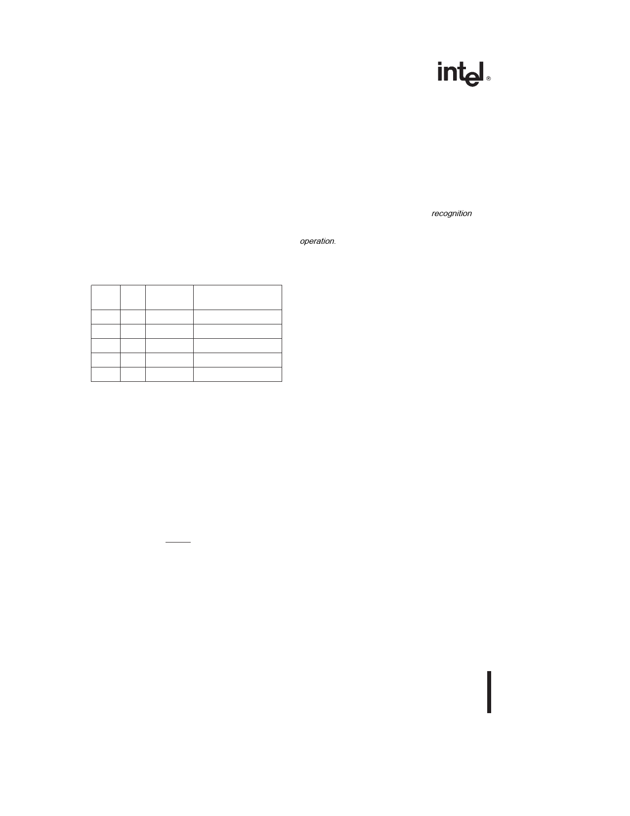
Prefix Identification
With the extended temperature range, operational
characteristics are guaranteed over the temperature
range corresponding to - 40°C to + 85°C ambient.
Package types are identified by a two-letter prefix to
the part number. The prefixes are listed in Table 1.
Table 1. Prefix Identification
Asynchronous pins require that setup and hold times
be met only in order to guarantee recognition at a
particular clock edge. Synchronous pins require that
setup and hold times be met to guarantee proper
operation. For example, missing the setup or hold
time for the SRDY pin (a synchronous input) will re-
sult in a system failure or lockup. Input pins may also
be edge- or level-sensitive. The possible character-
istics for input pins are S(E), S(L), A(E) and A(L).
Prefix Note
Package
Type
Temperature
Type
XX 1 PLCC
Extended
XX 1 QFP (EIAJ) Extended
XX 1, 2 SQFP
Extended/Commercial
X 1, 2 PLCC
Commercial
X 1, 2 QFP (EIAJ) Commercial
The Output States column indicates the output
state as a function of the device operating mode.
Output states are dependent upon the current activi-
ty of the processor. There are four operational
states that are different from regular operation: bus
hold, reset, Idle Mode and Powerdown Mode. Ap-
propriate characteristics for these states are also in-
dicated in this column, with the legend for all possi-
ble characteristics in Table 2.
NOTE:
1. To address the fact that many of the package prefix variables
have changed, all package prefix variables in this document
are now indicated with an "x".
2. The 5V 25 MHz and 3V 16 MHz versions are only avail-
able in commercial temperature range corresponding to
0°C to a 70°C ambient.
Pin Descriptions
Each pin or logical set of pins is described in Table
3. There are three columns for each entry in the Pin
Description Table.
The Pin Description column contains a text de-
scription of each pin.
As an example, consider AD15.0. I/O signifies the
pins are bidirectional. S(L) signifies that the input
function is synchronous and level-sensitive. H(Z)
signifies that, as outputs, the pins are high-imped-
ance upon acknowledgement of bus hold. R(Z) sig-
nifies that the pins float during reset. P(X) signifies
that the pins retain their states during Powerdown
Mode.
The Pin Name column contains a mnemonic that
describes the pin function. Negation of the signal
name (for example, RESIN) denotes a signal that is
active low.
8
Share Link: 