MMBT3906(2010) 查看數據表(PDF) - Micro Commercial Components
零件编号
产品描述 (功能)
生产厂家
MMBT3906 Datasheet PDF : 5 Pages
| |||
MCC
TM
Micro Commercial Components
omponents
20736 Marilla Street Chatsworth
!"#
$%
!"#
MMBT3906
Features
• Lead Free Finish/RoHS Compliant ("P" Suffix designates
RoHS Compliant. See ordering information)
• Case Material:Molded Plastic. UL Flammability
Classification Rating 94V-0 and MSL Rating 1
• Capable of 300mWatts of Power Dissipation
• Marking:2A
Maximum Ratings
Symbol
Rating
Rating
Unit
VCEO Collector-Emitter Voltage
-40
V
VCBO
VEBO
IC
PD
TJ
TSTG
Collector-Base Voltage
Emitter-Base Voltage
Collector Current, Continuous
Power Dissipation
Operating Junction Temperature
Storage Temperature
-40
V
-5.0
V
-0.2
A
0.3
W
-55 to +150
OC
-55 to +150
OC
Electrical Characteristics @ 25OC Unless Otherwise Specified
Symbol
Parameter
Min Max Units
V(BR)CEO
Collector-Emitter Breakdown Voltage*
(IC=-1.0mAdc, IB=0)
V(BR)CBO
V(BR)EBO
Collector-Base Breakdown Voltage
(IC=-10µAdc, IE=0)
Emitter-Base Breakdown Voltage
(IE=-10µAdc, IC=0)
IcBO
Collector cut-off Current
(VCB=-40Vdc, IE=0
ICEX
Collector Cut-off Current
(VCE=-30Vdc, VBE=-3.0Vdc)
IEBO
Emitter cut-off Current
(VEB=-5Vdc, IC=0
hFE
DC Current Gain*
(IC=-10mAdc, VCE=-1.0Vdc)
(IC=-50mAdc, VCE=-1.0Vdc)
(IC=-100mAdc, VCE=-1.0Vdc)
VCE(sat)
Collector-Emitter Saturation Voltage
(IC=-10mAdc, IB=-1.0mAdc)
(IC=-50mAdc, IB=-5.0mAdc)
VBE(sat)
Base-Emitter Saturation Voltage
(IC=-10mAdc, IB=-1.0mAdc)
(IC=-50mAdc, IB=-5.0mAdc)
Cobo
Outpuut Capacitance
(VCB=-5.0Vdc, f=1.0MHz,IE=0)
Cibo
Inpuut Capacitance
(VEB=-0.5Vdc, f=1.0MHz,IC=0)
fT
Current Gain-Bandwidth Product
(IC=-10mAdc, VCE=-20Vdc, f=100MHz)
NF
Noise Figure
(VCE=-5.0V, f=1.0kHz,IC=-100uA,Rs=1.0K)
SWITCHING CHARACTERISTICS
-40
-40
-5.0
100
60
30
-0.65
250
Vdc
Vdc
Vdc
-0.1
uAdc
-50
nAdc
-0.1
uAdc
300
-0.25 Vdc
-0.4
-0.85 Vdc
-0.95
4.5
pF
10
pF
MHz
4.0
dB
td
Delay Time
(VCC=-3.0Vdc, VBE=-0.5Vdc
tr
Rise Time
IC=-10mAdc, IB1=-1.0mAdc)
ts
Storage Time (VCC=-3.0Vdc, IC=-10mAdc
tf
Fall Time
IB1=IB2=-1.0mAdc )
*Pulse Width ≤ 300µs, Duty Cycle ≤ 2.0%
35
ns
35
ns
225
ns
75
ns
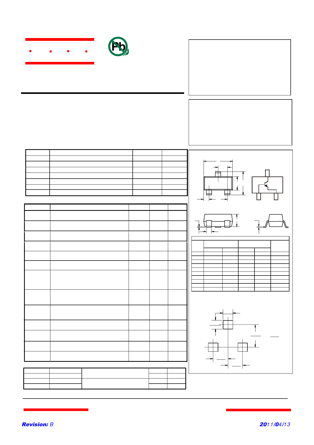
PNP General
Purpose Amplifier
SOT-23
A
D
C
CB
F
E
B
E
G
H
J
K
DIMENSIONS
INCHES
DIM
MIN
MAX
A
.110
.120
B
.083
.098
C
.047
.055
D
.035
.041
E
.070
.081
F
.018
.024
G
.0005
.0039
H
.035
.044
J
.003
.007
K
.015
.020
MM
MIN
2.80
2.10
1.20
.89
1.78
.45
.013
.89
.085
.37
MAX
3.04
2.64
1.40
1.03
2.05
.60
.100
1.12
.180
.51
NOTE
Suggested Solder
Pad Layout
.031
.800
.035
.900
.079
2.000
inches
mm
.037
.950
.037
.950
Revision: 9
www.mccsemi.com
1 of 5
2010/06/24
Share Link: 