LC73881M 查看數據表(PDF) - SANYO -> Panasonic
零件编号
产品描述 (功能)
生产厂家
LC73881M Datasheet PDF : 6 Pages
| |||
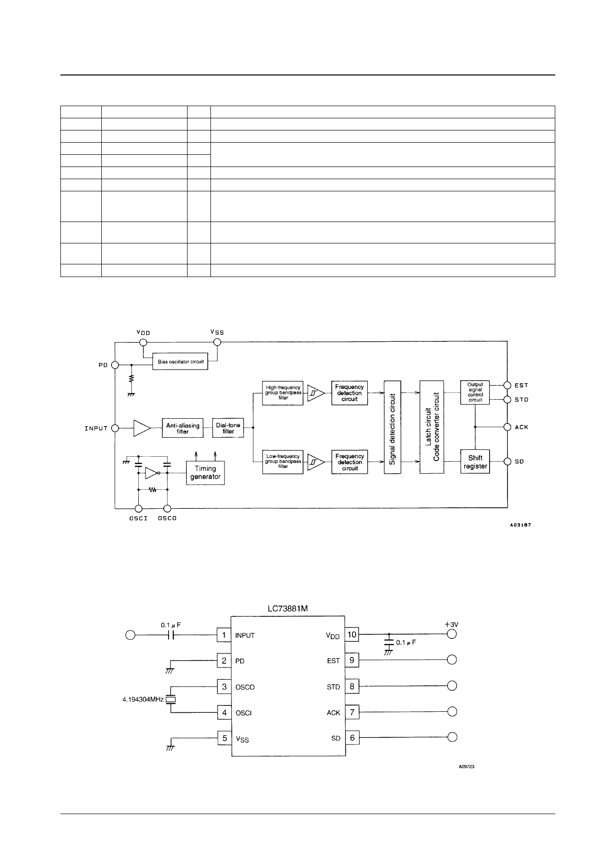
Pin Functions
Pin No.
1
2
3
4
5
6
Symbol
INPUT
PD
OSCO
OSCI
VSS
SD
7
ACK
8
STD
9
EST
10
VDD
Block Diagram
LC73881M
I/O
Function
I The input must be capacitor coupled. This signal is biased to VDD/2 internally.
I The LC73881M goes to low power mode when this pin is set high.
O Connect a 4.194304 MHz crystal oscillator or ceramic resonator to these pins to from an oscillator circuit.
I When using a ceramic resonator, a capacitor of approximately 30 pF must be connected to each pin.
Power supply pin. Normally 0 V.
O The decoded DTMF signal is output, this pin in a 4-bit LSB first format.
The ACK pin is used to shift out data from the SD pin. Four pulses are required to shift out the DTMF
I character, which consists of four bits. The rising edge of the first pulse latches the data (before shifting)
into the shift register.
A high level indicates the presence of a DTMF signal. Although the rise of this signal is later than that of the
O EST pin, it is less sensitive to burst waveforms and other noise.
A high level indicates the presence of a DTMF signal. Applications should monitor this pin and, after waiting
O an appropriate period, apply four pulses to the ACK pin to access the data.
Power supply pin. Normally 2.7 to 5.5 V.
Test Circuit, Sample Application Circuit
No. 5000-3/6
Share Link: 