16TTS08STRRPBF 查看數據表(PDF) - Vishay Semiconductors
零件编号
产品描述 (功能)
生产厂家
16TTS08STRRPBF Datasheet PDF : 7 Pages
| |||
16TTS..S High Voltage Series
Vishay High Power Products Surface Mountable Phase
Control SCR, 16 A
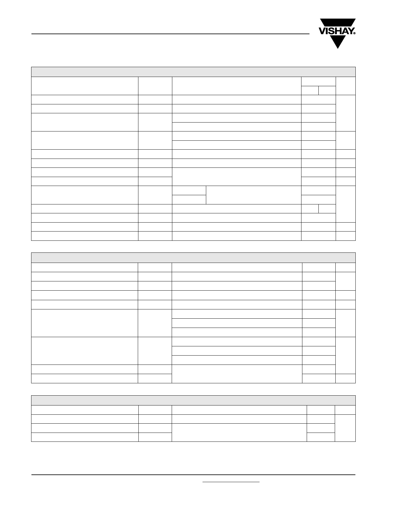
ABSOLUTE MAXIMUM RATINGS
PARAMETER
SYMBOL
TEST CONDITIONS
Maximum average on-state current
Maximum RMS on-state current
Maximum peak, one-cycle,
non-repetitive surge current
IT(AV)
IRMS
ITSM
Maximum I2t for fusing
I2t
Maximum I2√t for fusing
Maximum on-state voltage drop
On-state slope resistance
Threshold voltage
Maximum reverse and direct leakage current
Holding current
Maximum latching current
Maximum rate of rise of off-state voltage
Maximum rate of rise of turned-on current
I2√t
VTM
rt
VT(TO)
IRM/IDM
IH
IL
dV/dt
dI/dt
TC = 98 °C, 180° conduction, half sine wave
10 ms sine pulse, rated VRRM applied
10 ms sine pulse, no voltage reapplied
10 ms sine pulse, rated VRRM applied
10 ms sine pulse, no voltage reapplied
t = 0.1 to 10 ms, no voltage reapplied
10 A, TJ = 25 °C
TJ = 125 °C
TJ = 25 °C
TJ = 125 °C
VR = Rated VRRM/VDRM
Anode supply = 6 V, resistive load, initial IT = 1 A
Anode supply = 6 V, resistive load
VALUES
UNITS
TYP. MAX.
10
16
A
170
200
144
A2s
200
2000
A2√s
1.4
V
24.0
mΩ
1.1
V
0.5
10
mA
- 100
200
500
V/µs
150
A/µs
TRIGGERING
PARAMETER
Maximum peak gate power
Maximum average gate power
Maximum peak positive gate current
Maximum peak negative gate voltage
SYMBOL
PGM
PG(AV)
+ IGM
- VGM
Maximum required DC gate current to trigger
IGT
Maximum required DC gate
voltage to trigger
VGT
Maximum DC gate voltage not to trigger
VGD
Maximum DC gate current not to trigger
IGD
TEST CONDITIONS
Anode supply = 6 V, resistive load, TJ = - 10 °C
Anode supply = 6 V, resistive load, TJ = 25 °C
Anode supply = 6 V, resistive load, TJ = 125 °C
Anode supply = 6 V, resistive load, TJ = - 10 °C
Anode supply = 6 V, resistive load, TJ = 25 °C
Anode supply = 6 V, resistive load, TJ = 125 °C
TJ = 125 °C, VDRM = Rated value
SWITCHING
PARAMETER
Typical turn-on time
Typical reverse recovery time
Typical turn-off time
SYMBOL
tgt
trr
tq
TJ = 25 °C
TJ = 125 °C
TEST CONDITIONS
VALUES
8.0
2.0
1.5
10
90
60
35
3.0
2.0
1.0
0.25
2.0
UNITS
W
A
V
mA
V
mA
VALUES UNITS
0.9
4
µs
110
www.vishay.com
2
For technical questions, contact: diodes-tech@vishay.com
Document Number: 93698
Revision: 04-Jul-08
Share Link: 