SC1101(2000) 查看數據表(PDF) - Semtech Corporation
零件编号
产品描述 (功能)
生产厂家
SC1101 Datasheet PDF : 8 Pages
| |||
VOLTAGE MODE PWM CONTROLLER
SC1101
February 29, 2000
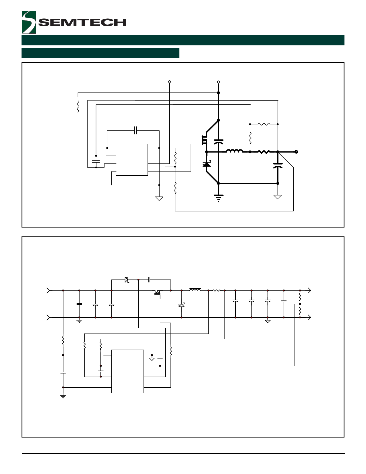
LAYOUT GUIDELINES
nection has fast voltage transitions, keeping this connec-
Careful attention to layout requirements are necessary tion short will minimize EMI. The connection between the
for successful implementation of the SC1101 PWM con- output inductor and the sense resistor should be a wide
troller. High currents switching at 200kHz are present in trace or copper area, there are no fast voltage or current
the application and their effect on ground plane voltage transitions in this connection and length is not so impor-
differentials must be understood and minimized.
tant, however adding unnecessary impedance will re-
duce efficiency.
1). The high power parts of the circuit should be laid out
first. A ground plane should be used, the number and 4) The Output Capacitor(s) (Cout) should be located as
position of ground plane interruptions should be such as close to the load as possible, fast transient load currents
to not unnecessarily compromise ground plane integrity. are supplied by Cout only, and connections between
Isolated or semi-isolated areas of the ground plane may Cout and the load must be short, wide copper areas to
be deliberately introduced to constrain ground currents minimize inductance and resistance.
to particular areas, for example the input capacitor and 5) The SC1101 is best placed over an isolated ground
bottom Schottky ground.
plane area. GND and PGND should be returned to this
2). The loop formed by the Input Capacitor(s) (Cin), the isolated ground. This isolated ground area should be
Top FET (Q1) and the Schottky (D1) must be kept as connected to the main ground by a trace that runs from
small as possible. This loop contains all the high current, the GND pin to the ground side of (one of) the output ca-
fast transition switching. Connections should be as wide pacitor(s). If this is not possible, the GND pin may be
and as short as possible to minimize loop inductance. connected to the ground path between the Output Ca-
Minimizing this loop area will reduce EMI, lower ground pacitor(s) and the Cin, Q1, D1 loop. Under no circum-
injection currents, resulting in electrically “cleaner”
stances should GND be returned to a ground inside the
grounds for the rest of the system and minimize source Cin, Q1, D1 loop.
ringing, resulting in more reliable gate switching signals. 6) Vcc for the SC1101 should be supplied from the 5V
3). The connection between the junction of Q1, D1 and supply through a 10Ω resistor, the Vcc pin should be de-
the output inductor should be a wide trace or copper re- coupled directly to GND by a 0.1µF ceramic capacitor,
gion. It should be as short as practical. Since this con- trace lengths should be as short as possible.
12V IN
5V
10
0.1uF
0.1uF
SC1101CS
1
VCC
8
GND
2
CS(-)
7
FB
3
6
CS(+) BST
4
PGND
5
DH
Heavy lines indicate
high current paths.
Fig. 5 Layout diagram for the SC1101
© 2000 SEMTECH CORP.
Q1
Cin +
1.00k
2.32k
Rb
D1
5mOhm
Vout
4uH
+
Cout
Ra
5
652 MITCHELL ROAD NEWBURY PARK CA 91320
Share Link: 