9014 查看數據表(PDF) - Fairchild Semiconductor
零件编号
产品描述 (功能)
生产厂家
9014 Datasheet PDF : 16 Pages
| |||
verter used to supply power to the microprocessor. Section 3-2 briefly explains the operation
of a Buck converter.
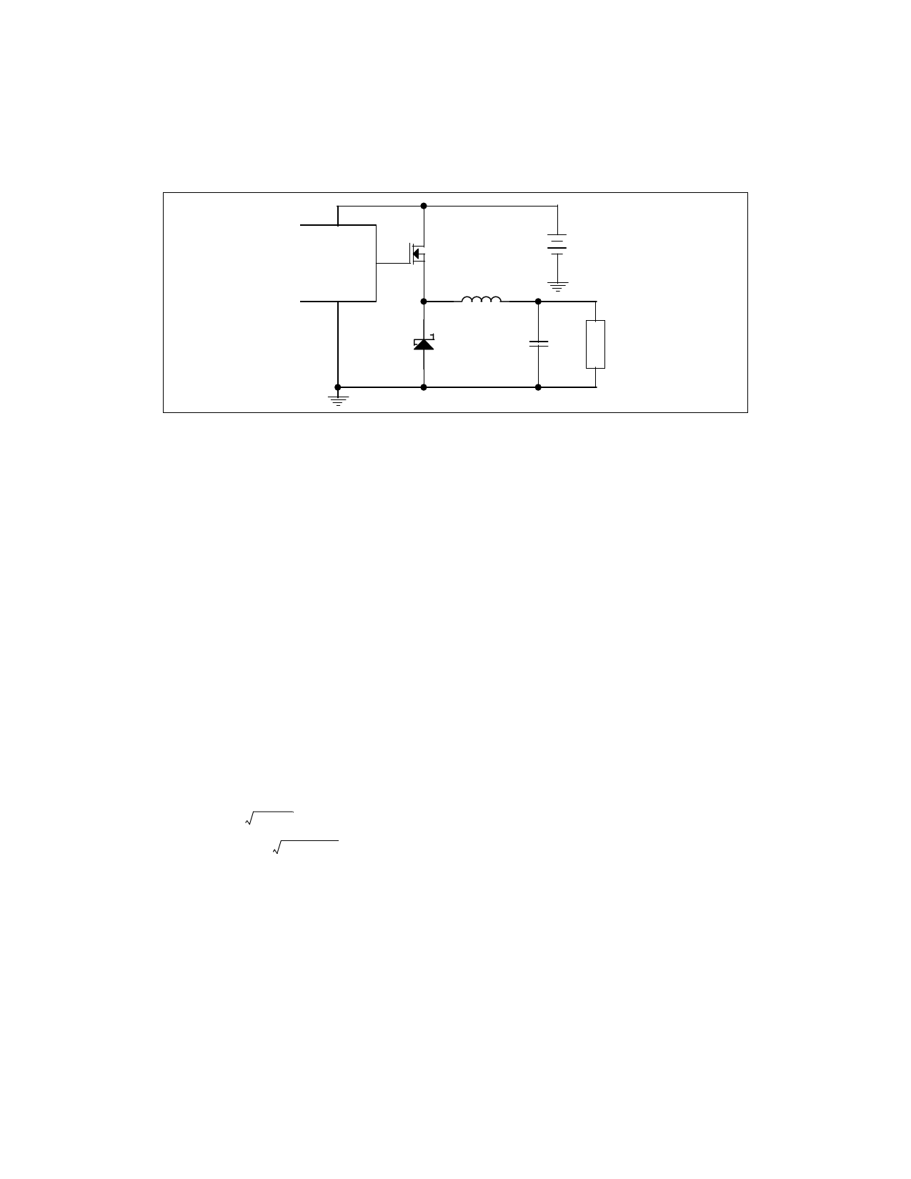
PWM
Control
IC
Switch MOSFET (Q1)
DC Input
(Vin)
(L2)
Freewheeling
Diode (D)
(C2) RL
Figure 3-1. Step-down (Buck) DC-DC Converter
3-1. Efficiency of Buck Converter
In order to increase the overall efficiency, it is important to reduce the loss generated in each
component, as much as possible, in low output voltage power supplies. Equation (3-11) in
Section 3-2 shows the reduction in system efficiency due to the loss associated with semicon-
ductor components such as the switch MOSFET (Q1) and freewheeling diode (D). If the free-
wheeling diode (D) is substituted with the MOSFET (Q2), the semiconductor component loss
can be reduced because the loss from the diode's forward voltage drop is greater than the loss
from the MOSFET’s RDS(on). This effect is represented by the following equation. First,
assume the following conditions: output current Iout=18[A], duty ratio D=0.49, freewheeling
(Schottky) diode's forward voltage drop VD=0.52[V] (the typical value when iF=18[A],
TJ=100[°C] in MBRD835L data sheet Figure 2), and MOSFET RDS(on)=14.70[mΩ] (the typical
value when VGS=10[V], TJ=100[°C] in Figure 2-3). Then, the freewheeling diode (D) loss can
be calculated by the following equation (3-1):
P = VDIout(1 – D)
= 0.52[V] × 18[A] × (1 – 0.49)………(3 – 1)
= 4.77[W]
If substituted with the MOSFET (Q2), the MOSFET (Q2) loss is calculated by equation (3-2) as
follows.
P = [Iout
(
1
–
D
2
)]
RDS(on)
= [18[A] ×
(
1
–
0.49
2
)]
×
14.70[
mΩ
]
…(
3
–
2
)
= 2.43[W]
The calculation results of equations (3-1) and (3-2) verify the increase in efficiency if the free-
wheeling diode (D) is substituted with a MOSFET(Q2). This method is called synchronous rec-
tification, and the MOSFET, a synchronous rectifier (Q2). Figure 3-2 is a remodeling of the
circuit shown in Figure 3-1 employing synchronous rectification. If the Schottky diode (D2) is
used in parallel with the synchronous rectifier (Q2) in this circuit, the inductor (L2) current that
previously flowed through the parasitic diode of the synchronous rectifier (Q2) starts flowing
through the faster and low loss Schottky diode (D2) during the switching dead time of the two
MOSFET’s (Q1, Q2). This flow pattern makes the circuit more efficient.
4
Rev. B, July 2000
Share Link: 