7228AIBIZ 查看數據表(PDF) - Renesas Electronics
零件编号
产品描述 (功能)
生产厂家
7228AIBIZ Datasheet PDF : 19 Pages
| |||
ICM7228
PIN NO.
NAME
9
HEXA/CODE
B/SHUTDOWN
10
DA2
11
ID1
12
ID0
13
ID2
14
ID3
15
DIGIT 1
16
DlGlT 2
17
DIGIT 5
18
DlGlT 8
19
VDD
20
DIGIT 4
21
DlGlT 7
22
DlGlT 6
23
DIGlT 3
24
SEG f
25
SEG d
26
SEG g
27
SEG a
28
VSS
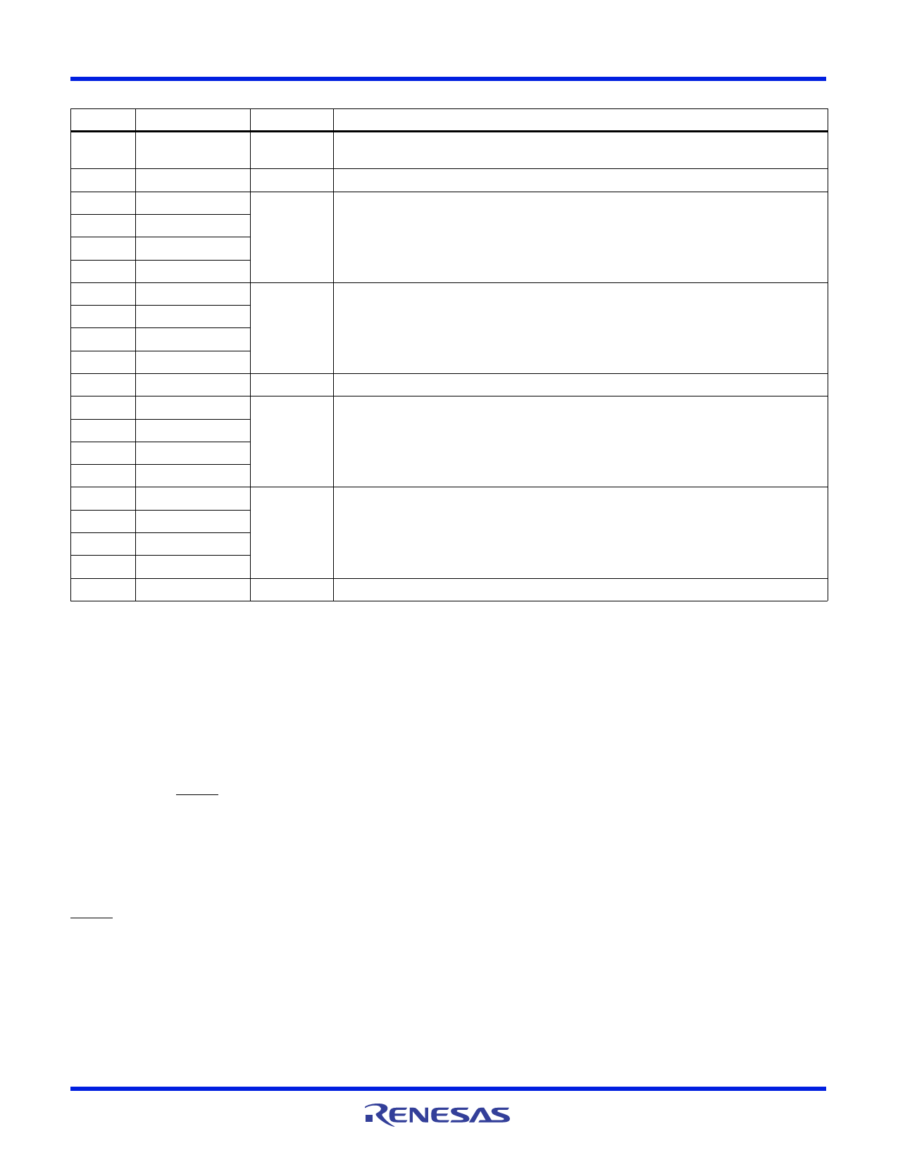
TABLE 3. ICM7228C PIN ASSIGNMENTS AND DESCRIPTIONS (Continued)
FUNCTION
DESCRIPTION
Input
Three Level Input. Display Function Control: High, Hexadecimal Decoding; Float, Code B
Decoding; Low, Oscillator, and Display Disabled.
Input
Digit Address Input, Bit 3, MSB.
Input
Display Data Inputs.
Output LED Display Digits 1, 2, 5 and 8 Drive Lines.
Supply
Output
Device Positive Power Supply Rail.
LED Display Digits 4, 7, 6 and 3 Drive Lines.
Output LED Display Segments f, d, g and a Drive Lines.
Supply Device Ground or Negative Power Supply Rail.
Detailed Description
System Interfacing and Data Entry Modes, ICM7228A
and ICM7228B
The ICM7228A/B devices are compatible with the architectures
of most microprocessor systems. Their fast switching
characteristics makes it possible to access them as a memory
mapped I/O device with no wait state necessary in most
microcontroller systems. All the ICM7228A/B inputs, including
MODE, feature a 250ns minimum setup and 0ns hold time with
a 200ns minimum WRITE pulse. Input logic levels are TTL and
CMOS compatible. Figure 9 shows a generic method of driving
the ICM7228A/B from a microprocessor bus. To the
microprocessor, each device appears to be 2 separate I/O
locations; the Control Register and the Display RAM. Selection
between the two is accomplished by the MODE input driven by
address line A0. Input data is placed on the lD0 - lD7 lines. The
WRITE input acts as both a device select and write cycle timing
pulse. See Figure 1 and Switching Specifications Table for write
cycle timing parameters.
The ICM7228A/B have three data entry modes: Control Register
update without RAM update, sequential 8-digit update and
single digit update. In all three modes a control word is first
written by pulsing the WRITE input while the MODE input is
high, thereby latching data into the Control Register. The logic
level of individual bits in the Control Register select Shutdown,
Decode/No Decode, Hex/Code B, RAM bank A/B and Display
RAM digit address as shown in Tables 1 and 2.
The ICM7228A/B Display RAM is divided into 2 banks, called
bank A and B. When using the Hexadecimal or code B display
modes, these RAM banks can be selected separately. This allows
two separate sets of display data to be stored and displayed
alternately. Notice that the RAM bank selection is not possible in
No-Decode mode, this is because the display data in the No-
Decode mode has 8 bits, but in Decoded schemes (Hex/Code B)
is only 4 bits (lD0 - lD3 data). It should also be mentioned that the
decimal point is independent of selected bank, a turned on
decimal point will remain on for either bank. Selection of the RAM
banks is controlled by lD3 input. The lD3 logic level (during
Control Register update) selects which bank of the internal RAM
to be written to and/or displayed.
Control Register Update without RAM Update
The Control Register can be updated without changing the display
data by a single pulse on the WRITE input, with MODE high and
DATA COMING low. If the display is being decoded (Hex/Code
B), then the value of lD3 determines which RAM bank will be
selected and displayed for all eight digits.
Sequential 8-Digit Update
FN3160 Rev 9.00
August 19, 2015
Page 11 of 19
Share Link: 