8533AG-01LF 查看數據表(PDF) - Integrated Device Technology
零件编号
产品描述 (功能)
生产厂家
8533AG-01LF Datasheet PDF : 17 Pages
| |||
8533-01 Data Sheet
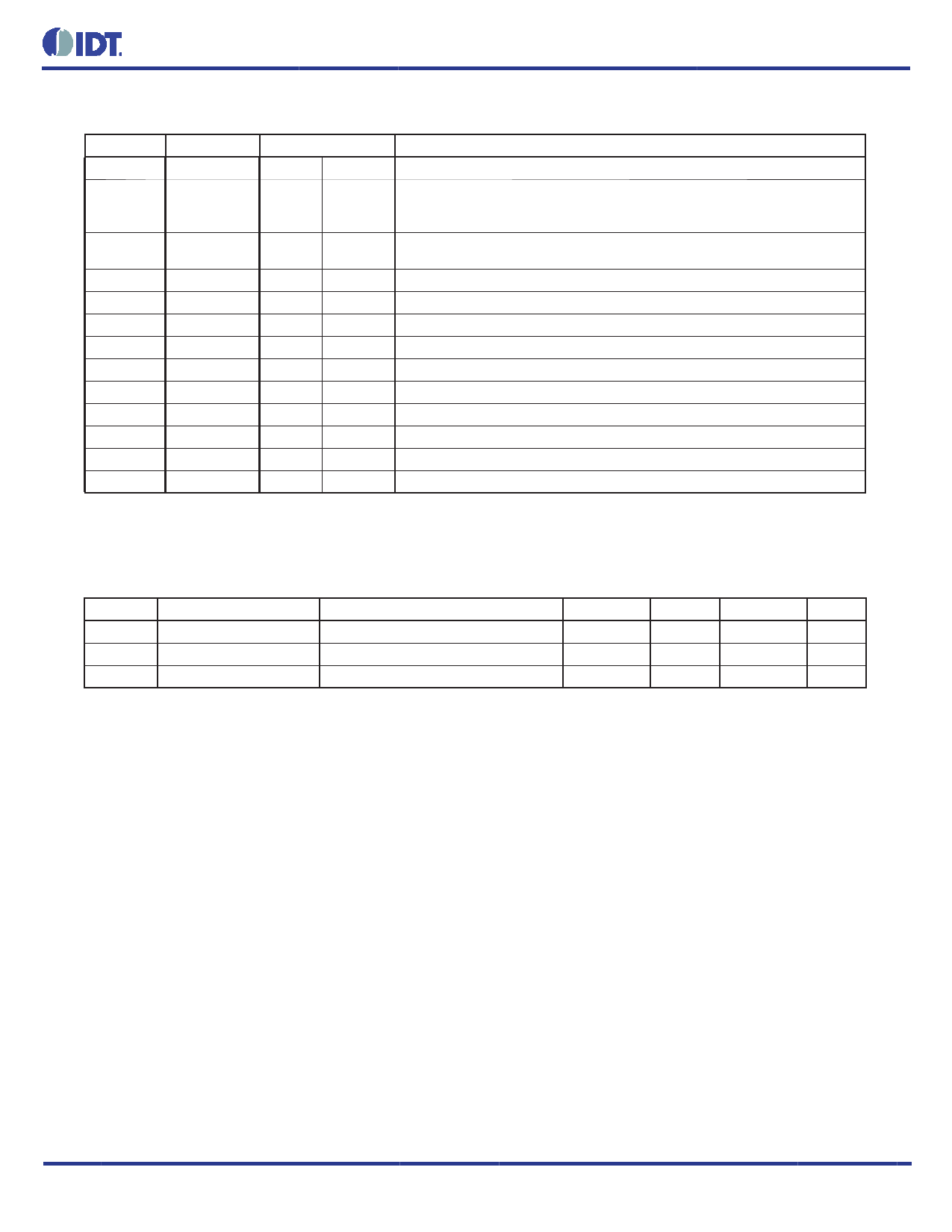
TABLE 1. PIN DESCRIPTIONS
Number
Name
Type
Description
1
VEE
Power
Negative supply pin.
Synchronizing clock enable. When HIGH, clock outputs follow clock input.
2
CLK_EN Input Pullup When LOW, Q outputs are forced low, nQ outputs are forced high. LVC-
MOS / LVTTL interface levels.
3
CLK_SEL
Input
Pulldown
Clock select input. When HIGH, selects differential PCLK, nPCLK inputs.
When LOW, selects CLK, nCLK inputs. LVCMOS / LVTTL interface levels.
4
CLK
Input Pulldown Non-inverting differential clock input.
5
nCLK
Input Pullup Inverting differential clock input.
6
PCLK
Input Pulldown Non-inverting differential LVPECL clock input.
7
nPCLK
Input Pullup Inverting differential LVPECL clock input.
8, 9
nc
Unused
No connect.
10, 13, 18
11, 12
VCC
nQ3, Q3
Power
Output
Positive supply pins.
Differential output pair. LVPECL interface levels.
14, 15
nQ2, Q2 Output
Differential output pair. LVPECL interface levels.
16, 17
nQ1, Q1 Output
Differential output pair. LVPECL interface levels.
19, 20
nQ0, Q0 Output
Differential output pair. LVPECL interface levels.
NOTE: Pullup and Pulldown refer to internal input resistors. See Table 2, Pin Characteristics, for typical values.
TABLE 2. PIN CHARACTERISTICS
Symbol Parameter
CIN
RPULLUP
RPULLDOWN
Input Capacitance
Input Pullup Resistor
Input Pulldown Resistor
Test Conditions
Minimum
Typical
4
51
51
Maximum
Units
pF
kΩ
kΩ
©2016 Integrated Device Technology, Inc
2
Revision F January 19, 2016
Share Link: 